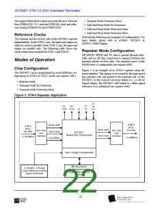
Functional Description
Updating the Transmit AU Pointer
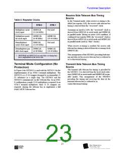
Transmit Side Telecom Bus Timing
Justification Event Counters
Source
If the re-timing function on the receive side is disabled,
re-clocking by the local clock will occur on the trans-
mit side of the SXT6051. If the receive and local
(which generates the transmit clock) clocks are
slightly different, pointer movements on the transmit
side of the SXT6051 will be generated. These pointer
movements will be reflected in the transmit AU
pointer justification event counters.
On the transmit side, the master SXT6051 feeds the
data received from its transmit telecom bus to both its
MST block and MSP block (which feeds the slave)
using a contra-directional timing arrangement at the
transmit telecom bus interface.
Co-directional timing arrangement is used in both the
receive and transmit directions at the MSP interface.
Receiver Default Operation
If the re-timing function is enabled, re-clocking will
take place on the receive side. Similarly, if the receive
and the local (which generates DRETCLK and trans-
mit clock) clocks are slightly different, pointer move-
ments are again generated on the transmit side of the
SXT6051 and reflected in transmit AU pointer justifi-
cation event counters.
Figure 7 is a block diagram of the receive section of the
SXT6051. The detailed description follows the data flow
from left to right and describes the functionality and con-
figuration of each block. Note that all status change alarms,
counter overflow alarms and receive byte change alarms
mentioned, can cause the INT output pin to be activated if
they are unmasked. Please refer to the register definition
for location of alarms, masks & interrupts.
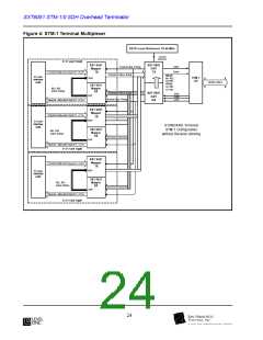
Terminal Protection Mode
Figure describes the dataflow for a 1-for-1 terminal protec-
tion configuration. The protection mode is an implementa-
tion of the ITU specifications in 1-for-1 configuration.
Serial Interface
The serial interface block accepts an STM-0 input as a
B3ZS encoded or NRZ signal. The B3ZS signal is
input at DHPOSD and DHNEGD and the NRZ signal
is input at DHPOSD. The 51.84 MHz clock is input at
DHICLK.
The SXT6051 can be used either in the main (master) or the
redundant (slave) signal path. The master & slave signal
paths are connected via the MSP bus.
In the master configuration the SXT6051 is connected to
the SXT6251 via the telecom bus in both the transmit and
the receive directions.
A bipolar violation detector has been implemented in
the B3ZS decoder. Detection of a BPV is indicated in
register A0H. Note that the selection (see register 50H)
of the serial interface and B3ZS encoder and decoder
is common to both the transmit and receive sides of the
chip.
In the slave configuration the SXT6051 is indirectly con-
nected to the SXT6251 via the MSP bus in both the trans-
mit and the receive directions.
A filter for the LOS input is provided by the line inter-
face circuit (register 40H). The filtering on the LOS
can be integrated over 128 or 4096 clock cycles. A
LOS status change is indicated in register A0H.
Receive Side Telecom Bus Timing
Source
On the receive side, the master SXT6051 selects the
data from either its receive MST block or its receive
MSP bus (fed by the slave) and presents this selection
using a co-directional timing arrangement at the
receive telecom bus interface. If the MSP (slave) data
is selected (i.e., the protection switch is active, see reg-
ister 21H) the clock provided at the receive telecom
bus will be derived from either DMSPPCKI (demulti-
plexer protection clock) or, if retiming is enabled,
DRETCLK (demultiplexer retiming clock, see register
51H).
Parallel Interface
The parallel interface block accepts a byte format input
at DHBDATA<7:0> in STM-0 or STM-1 mode. No
specific order on the byte is required for the SXT6051
to operate. The parallel clock is input at DHBCLK. As
in the serial case, the selection (see register 50H) of a
parallel interface is common between transmit and
receive sides.
A filter for the LOS input is provided by the line inter-
face circuit. The filtering on the LOS can be integrated
over 16 or 512 clock cycles. An LOS status change is
indicated in register A0H.
26
l

 LevelOne [ LEVEL ONE ]