ST150S
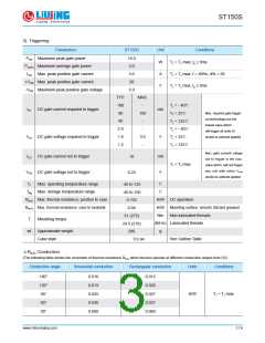
3). Triggering
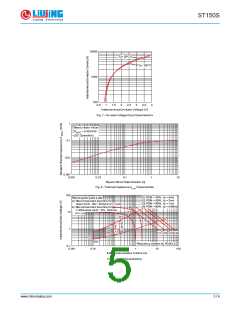
Parameters
ST150S
10.0
2.0
Unit
W
A
Conditions
PGM Maximum peak gate power
TJ = TJ max, tp ≤ 5ms
PG(AV) Maximum average gate power
IGM Max. peak positive gate current
+VGM Max. peak positive gate current
-VGM Maximum peak positive gate voltage
3.0
TJ = TJ max, f = 50Hz, d% = 50
20
V
TJ = TJ max, tp ≤ 5ms
5.0
TYP.
180
90
MAX.
℃
-
150
-
TJ = - 40
IGT
DC gate current required to trigger
mA
℃
Max. required gate trigger
TJ = 25
current/voltage are the
lowest value which
℃
℃
40
TJ = 125
2.9
1.8
1.2
-
TJ = - 40
will trigger all units 6V
anode-to-cathode applied
℃
3.0
-
VGT DC gate voltage required to trigger
V
TJ = 25
℃
TJ = 125
Max. gate current/ voltage
not to trigger is the max.
value which. will not trigger
any unit with rated VDRM
anode-to-cathode applied
IGD
DC gate current not to trigger
mA
V
10
TJ = TJ max.
VGD DC gate voltage not to trigger
0.25
℃
℃
TJ
Max. operating temperature range
Max. storage temperature range
-40 to 125
-40 to 150
0.105
T
stg
RthJC Max. thermal resistance, junction to case
RthCS Max. thermal resistance, case to heatsink
K/W DC operation
K/W Mounting surface, smooth, flat and greased
Nm
Non lubricated threads
0.04
31 (275)
24.5 (210)
280
T
Mounting torque
(lbf-in) Lubricated threads
wt
Approximate weight
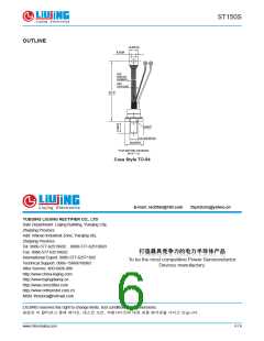
Case style
g
See Outline Table
TO-94
Δ
RthJC Conduction
(The following table shows the increment of thermal resistence RthJC when devices operate at different conduction angles than DC)
Conduction angle
Sinusoidal conduction
Rectangular conduction
Units
Conditions
°
°
180
0.016
0.019
0.025
0.036
0.060
0.012
0.020
0.027
0.037
0.060
120
°
K/W
TJ = TJ max.
90
60
30
°
°
www.china-liujing.com
3 / 6

 LIUJING [ 浙江柳晶整流器有限公司 ]