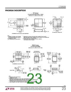
LT3505
APPLICATIONS INFORMATION
ing the total power loss from an efficiency measurement
and subtracting the catch diode loss. Thermal resistance
depends on the layout of the circuit board, but 43°C/W is
typical for the (3mm × 3mm) DFN (DD) package.
systemgroundinonlyoneplace.Thesecomponents,along
with the inductor and output capacitor, should be placed
onthesamesideofthecircuitboardandtheirconnections
shouldbemadeonthatlayer.Placealocal,unbrokenground
plane below these components and tie this ground plane
to system ground at one location, ideally at the ground
terminal of the output capacitor C1. The SW and BOOST
nodes should be as small as possible. Finally, keep the
FB node small so that the ground pin and ground traces
will shield it from the SW and BOOST nodes. Include vias
near the exposed GND pad of the LT3505 to help remove
heat from the LT3505 to the ground plane.
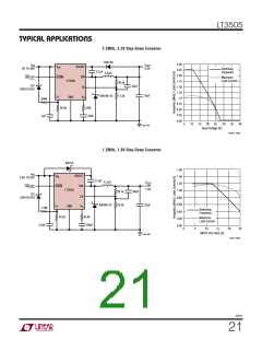
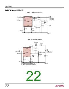
Outputs Greater Than 6V
For outputs greater than 6V, add a 1k to 2.5k resistor
across the inductor to damp the discontinuous ringing
of the SW node, preventing unintended SW current. The
12V Step-Down Converter circuit in the Typical Applica-
tions section shows the location of this resistor. Also note
that for outputs above 10V, the input voltage range will
be limited by the maximum rating of the BOOST pin. The
12V circuit shows how to overcome this limitation using
an additional zener diode.
High Temperature Considerations
The die temperature of the LT3505 must be lower than the
maximum rating of 125°C. This is generally not a concern
unless the ambient temperature is above 85°C. For higher
temperatures, care should be taken in the layout of the
circuit to ensure good heat sinking of the LT3505. The
maximum load current should be derated as the ambient
temperature approaches 125°C. The die temperature is
calculated by multiplying the LT3505 power dissipation
bythethermalresistancefromjunctiontoambient. Power
dissipationwithintheLT3505canbeestimatedbycalculat-
Other Linear Technology Publications
Application notes AN19, AN35 and AN44 contain more
detailed descriptions and design information for Buck
regulators and other switching regulators. The LT1376
data sheet has a more extensive discussion of output
ripple, loop compensation and stability testing. Design
Note DN100 shows how to generate a bipolar output
supply using a Buck regulator.
3505fc
20

 Linear [ Linear ]