LT3505
APPLICATIONS INFORMATION
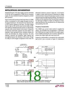
damaging the part. If the input supply is poorly controlled
or the user will be plugging the LT3505 into an energized
supply, the input network should be designed to prevent
this overshoot.
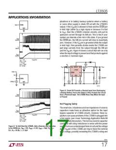
alternative solution is shown in Figure 9c. A 1Ω resistor
is added in series with the input to eliminate the voltage
overshoot (it also reduces the peak input current). A 0.1µF
capacitorimproveshighfrequencyfiltering.Thissolutionis
smaller and less expensive than the electrolytic capacitor.
For high input voltages its impact on efficiency is minor,
reducing efficiency only one percent for a 5V output at full
load operating from 24V.
Figure10showsthewaveformsthatresultwhenanLT3505
circuit is connected to a 24V supply through six feet of
24-gauge twisted pair. The first plot is the response with
a 2.2µF ceramic capacitor at the input. The input voltage
rings as high as 35V and the input current peaks at 20A.
One method of damping the tank circuit is to add another
capacitor with a series resistor to the circuit. In Figure 9b
an aluminum electrolytic capacitor has been added. This
capacitor’s high equivalent series resistance damps the
circuit and eliminates the voltage overshoot. The extra
capacitor improves low frequency ripple filtering and
can slightly improve the efficiency of the circuit, though
it is likely to be the largest component in the circuit. An
Frequency Compensation
The LT3505 uses current mode control to regulate the
output. This simplifies loop compensation. In particular,
the LT3505 does not require the ESR of the output capaci-
tor for stability allowing the use of ceramic capacitors to
achieve low output ripple and small circuit size.
Frequency compensation is provided by the components
tied to the VC pin, as shown in Figure 10. Generally a
CLOSING SWITCH
SIMULATES HOT PLUG
I
IN
V
IN
DANGER!
LT3505
2.2µF
V
IN
20V/DIV
RINGING V MAY EXCEED
IN
ABSOLUTE MAXIMUM
RATING OF THE LT3505
+
I
IN
5A/DIV
LOW
STRAY
IMPEDANCE
ENERGIZED
24V SUPPLY
INDUCTANCE
DUE TO 6 FEET
(2 METERS) OF
TWISTED PAIR
20µs/DIV
(9a)
V
LT3505
2.2µF
IN
20V/DIV
+
+
+
10µF
35V
AI.EI.
I
IN
5A/DIV
(9b)
20µs/DIV
1Ω
V
LT3505
2.2µF
IN
20V/DIV
0.1µF
I
IN
5A/DIV
3505 F10
20µs/DIV
(9c)
Figure 10. A Well Chosen Input Network Prevents Input Voltage Overshoot and
Ensures Reliable Operation When the LT3505 is Connected to a Live Supply
3505fc
18

 Linear [ Linear ]