LT3505
APPLICATIONS INFORMATION
capacitor (CC) and a resistor (RC) in series to ground are
used. In addition, a lower value filter capacitor (CF) may be
addedinparallel.Thefiltercapacitorisnotapartoftheloop
compensation but is used to filter noise at the switching
frequency, and is required only if a phase-lead capacitor
is used or if the output capacitor has high ESR.
CURRENT MODE
POWER STAGE
LT3505
–
0.8V
SW
g
=
m
OUT
1.1A/V
+
C
R1
PL
–
+
FB
g
=
V
m
C
200µA/V
ESR
780mV
C1
ERROR
+
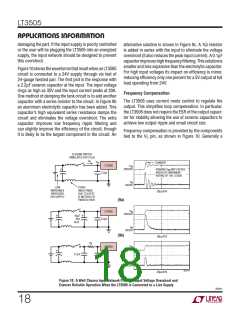
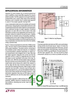
Loop compensation determines the stability and transient
performance.Designingthecompensationnetworkisabit
complicatedandthebestvaluesdependontheapplication
and in particular the type of output capacitor. A practical
approach is to start with one of the circuits in this data
sheet that is similar to your application and tune the com-
pensation network to optimize the performance. Stability
should then be checked across all operating conditions,
includingloadcurrent, inputvoltageandtemperature. The
LT1375datasheetcontainsamorethoroughdiscussionof
loop compensation and describes how to test the stability
using a transient load.
AMPLIFIER
2M
C1
R2
R
C
C
C
C
F
3505 F11
Figure 11. Model for Loop Response
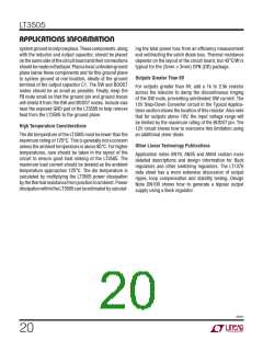
PCB Layout
ForproperoperationandminimumEMI,caremustbetaken
during printed circuit board layout. Figure 12 shows the
recommended component placement with trace, ground
plane and via locations. Note that large, switched currents
flow in the LT3505’s VIN and SW pins, the catch diode (D1)
and the input capacitor (C2). The loop formed by these
components should be as small as possible and tied to
Figure11showsanequivalentcircuitfortheLT3505control
loop. The error amp is a transconductance amplifier with
finite output impedance. The power section, consisting of
the modulator, power switch and inductor, is modeled as
a transconductance amplifier generating an output cur-
rent proportional to the voltage at the VC node. Note that
the output capacitor integrates this current and that the
capacitor on the VC node (CC) integrates the error ampli-
fier output current, resulting in two poles in the loop. RC
provides a zero. With the recommended output capacitor,
theloopcrossoveroccursabovetheRCCCzero.Thissimple
model works well as long as the value of the inductor is
not too high and the loop crossover frequency is much
lower than the switching frequency. With a larger ceramic
capacitor (very low ESR), crossover may be lower and a
phaseleadcapacitor(CPL)acrossthefeedbackdividermay
improve the phase margin and transient response. Large
electrolytic capacitors may have an ESR large enough to
create an additional zero and the phase lead may not be
necessary.
SYSTEM
V
GROUND OUT
: VIAS TO LOCAL GROUND PLANE
: OUTLINE OF LOCAL GROUND PLANE
C1
V
OUT
BOOST
SW
1
8
7
6
5
V
C
FB
2
3
4
R
T
D1
C2
POWER
GROUND
SIGNAL
GROUND
If the output capacitor is different than the recommended
capacitor, stability should be checked across all operat-
ing conditions, including load current, input voltage and
temperature.
3505 F12
V
IN
SHUTDOWN
Figure 12. A Good PCB Layout Ensures Proper, Low EMI Operation
3505fc
19

 Linear [ Linear ]