LT3505
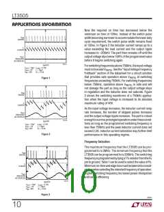
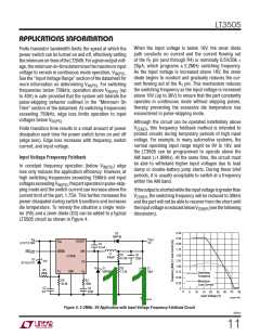
APPLICATIONS INFORMATION
twice its nominal value, possibly exceeding the LT3505’s
voltage rating. This situation can be easily avoided; see
the Hot Plugging Safely section.
High performance electrolytic capacitors can be used for
theoutputcapacitor. LowESRisimportant, sochooseone
that is intended for use in switching regulators. The ESR
should be specified by the supplier and should be 0.1Ω
or less. Such a capacitor will be larger than a ceramic
capacitor and will have a larger capacitance, because the
capacitor must be large to achieve low ESR. Table 3 lists
several capacitor vendors.
Output Capacitor
The output capacitor has two essential functions. Along
with the inductor, it filters the square wave generated by
the LT3505 to produce the DC output. In this role it deter-
mines the output ripple so low impedance at the switching
frequency is important. The second function is to store
energy in order to satisfy transient loads and stabilize the
LT3505’s control loop.
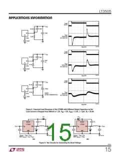
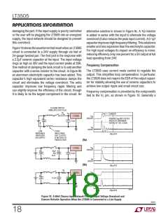
Figure 5 shows the transient response of the LT3505 with
several output capacitor choices. The output is 3.3V. The
load current is stepped from 500mA to 1.2A and back
to 500mA and the oscilloscope traces show the output
voltage. The upper photo shows the recommended value.
The second photo shows the improved response (less
voltage drop) resulting from a larger output capacitor
and a larger phase lead capacitor. The last photo shows
the response to a high performance electrolytic capaci-
tor. Transient performance is improved due to the large
output capacitance.
Ceramic capacitors have very low equivalent series re-
sistance (ESR) and provide the best ripple performance.
A good value is:
COUT = 49/(VOUT • fSW
)
where COUT is in µF and fSW is in MHz. Use X5R or X7R
types and keep in mind that a ceramic capacitor biased
with VOUT will have less than its nominal capacitance. This
choice will provide low output ripple and good transient
response. Transient performance can be improved with a
high value capacitor, if the compensation network is also
adjusted to maintain the loop bandwidth.
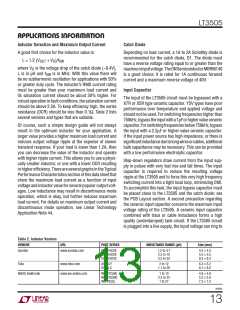
BOOST Pin Considerations
Capacitor C3 and diode D2 are used to generate a boost
voltage that is higher than the input voltage. In most cases
a 0.1µF capacitor and fast switching diode (such as the
1N4148 or 1N914) will work well. Figure 6 shows two
ways to arrange the boost circuit. The BOOST pin must
be at least 2.3V above the SW pin for best efficiency. For
outputs of 3.3V and above, the standard circuit (Figure 6a)
is best. For outputs between 3V and 3.3V, use a 0.22µF
capacitor. For outputs between 2.5V and 3V, use a 0.47µF
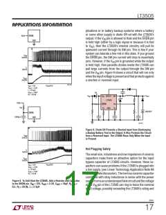
A lower value of output capacitor can be used, but tran-
sient performance will suffer unless the compensation
network is adjusted to reduce the loop gain. Also, a lower
value output capacitor may result in increased sensitivity
to noise which can be alleviated by adding a 22pF phase
lead capacitor from FB to VOUT
.
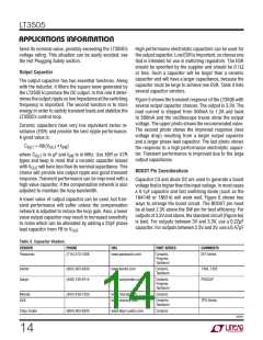
Table 3. Capacitor Vendors
VENDOR
PHONE
URL
PART SERIES
COMMENTS
Panasonic
(714) 373-7366
www.panasonic.com
Ceramic,
Polymer,
Tantalum
EEF Series
Kemet
Sanyo
(864) 963-6300
(408) 749-9714
www.kemet.com
Ceramic,
Tantalum
T494, T495
POSCAP
www.sanyovideo.com
Ceramic,
Polymer,
Tantalum
Murata
AVX
(404) 436-1300
(864) 963-6300
www.murata.com
www.avxcorp.com
Ceramic
Ceramic,
Tantalum
TPS Series
Taiyo Yuden
www.taiyo-yuden.com
Ceramic
3505fc
14

 Linear [ Linear ]