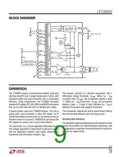
LTC6820
elecTrical characTerisTics The l denotes the specifications which apply over the full specified
temperature range, otherwise specifications are at TA = 25°C. VDD = 2.7V to 5.5V, VDDS = 1.7V to 5.5V, RBIAS = 2k to 20k unless
otherwise specified. All voltages are with respect to GND.
SYMBOL PARAMETER
Power Supply
CONDITIONS
MIN
TYP
MAX
UNITS
l
l
l
V
V
Operating Supply Voltage Range
IO Supply Voltage Range (Level Shifting)
Supply Current, READY/ACTIVE States
(Note 4)
2.7
1.7
4
5.5
5.5
5.8
V
V
mA
mA
DD
Affects CS, SCK, MOSI, MISO and EN Pins
DDS
I
R
= 2kΩ (I = 1mA)
1/t
1/t
= 0MHz
= 1MHz
4.8
7
DD
BIAS
B
CLK
CLK
l
R
= 20kΩ (I = 0.1mA)
1/t
1/t
= 0MHz
= 1MHz
1.3
2
2.4
2.9
mA
mA
BIAS
B
CLK
CLK
l
l
Supply Current, IDLE State
IO Supply Current (Note 5)
MSTR = 0V
MSTR = V
SPI Inputs and EN Pin at 0V or V
SPI Outputs Unloaded
2
1
6
3
1
µA
µA
µA
DD
l
I
,
DDS
DDS
Biasing
l
l
V
Voltage on IBIAS Pin
READY/ACTIVE State
IDLE State
1.9
2.0
0
2.1
V
V
mA
BIAS
I
Isolated Interface Bias Current (Note 6)
Isolated Interface Current Gain
R
= 2k to 20k
V
/R
B
BIAS
BIAS BIAS
l
l
A
V
V
V ≤ 1.6V
A
I = 1mA
B
18
18
20
20
22
24
mA/mA
mA/mA
IB
B
I = 0.1mA
l
l
Transmitter Pulse Amplitude
V = |V – V
|
IM
V
V
< 3.3V
≥ 3.3V
V
– 1.7V
DD
1.6
V
V
V
µA
µA
V/V
A
A
IP
DD
DD
l
l
l
l
Threshold-Setting Voltage on ICMP Pin
Leakage Current on ICMP Pin
Leakage Current on IP and IM Pins
Receiver Comparator Threshold Voltage
Gain
V
V
= A
= 0V to V
• V
0.2
0.4
1.5
1
2
ICMP
TCMP
ICMP
TCMP
ICMP
I
LEAK(ICMP)
DD
I
IDLE State, V = V = 0V to V
DD
LEAK(IP/IM)
IP
IM
A
V
V
= V /2 to V – 0.2V,
ICMP
0.5
0.6
TCMP
CM
DD
DD
= 0.2V to 1.5V
V
R
Receiver Common Mode Bias
Receiver Input Resistance
IP/IM Not Driving
Single-Ended to IP or IM
(V – V
26
/3 – 167mV)
ICMP
V
kΩ
CM
DD
l
l
35
42
IN
Idle/Wake-Up (See Figures 13, 14, 15)
V
Differential Wake-Up Voltage
(See Figure 13)
t
= 240ns
DWELL
240
240
mV
WAKE
l
l
l
t
t
t
Dwell Time at V
V
= 240mV
WAKE
ns
µs
ms
DWELL
READY
IDLE
WAKE
Start-Up Time After Wake Detection
Idle Time-Out Duration
8
4
5.7
7.5
Digital I/O
l
l
V
V
V
V
V
V
V
V
Digital Voltage Input High, Configuration
Pins (PHA, POL, MSTR, SLOW)
Digital Voltage Input Low, Configuration
Pins (PHA, POL, MSTR, SLOW)
Digital Voltage Input High, SPI Pins
(CS, SCK, MOSI, MISO)
V
V
= 2.7V to 5.5V (POL, PHA, MSTR, SLOW)
= 2.7V to 5.5V (POL, PHA, MSTR, SLOW)
0.7 • V
V
V
IH(CFG)
IL(CFG)
IH(SPI)
IL(SPI)
IH(EN)
IL(EN)
OH
DD
DD
DD
0.3 • V
DD
l
l
V
V
V
V
V
V
V
V
V
V
V
V
= 2.7V to 5.5V
= 1.7V to 2.7V
0.7 • V
0.8 • V
V
V
V
V
V
V
V
V
V
V
V
V
DDS
DDS
DDS
DDS
l
l
Digital Voltage Input Low, SPI Pins
(CS, SCK, MOSI, MISO)
= 2.7V to 5.5V
= 1.7V to 2.7V
0.3 • V
0.2 • V
DDS
DDS
DDS
DDS
l
l
Digital Voltage Input High, EN Pin
Digital Voltage Input Low, EN Pin
Digital Voltage Output High (CS and SCK)
= 2.7V to 5.5V
= 1.7V to 2.7V
2
DDS
DDS
0.85 • V
DDS
l
l
= 2.7V to 5.5V
= 1.7V to 2.7V
0.8
DDS
DDS
0.25 • V
DDS
l
l
= 3.3V, Sourcing 2mA
= 1.7V, Sourcing 1mA
V
– 0.2
– 0.25
DDS
DDS
DDS
DDS
V
l
l
Digital Voltage Output Low
(MOSI, MISO, CS, SCK)
= 3.3V, Sinking 3.3mA
= 1.7V, Sinking 1mA
0.2
0.2
OL
DDS
DDS
6820f
3

 Linear [ Linear ]