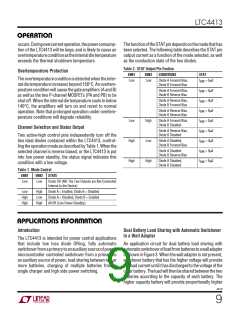
LTC4413
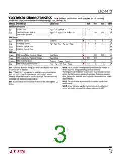
ELECTRICAL CHARACTERISTICS
The ● indicates specifications which apply over the full operating
temperature range, otherwise specifications are at TA = 25°C. (Notes 2, 6)
SYMBOL PARAMETER
Short-Circuit Response
CONDITIONS
MIN
TYP
MAX
UNITS
I
I
Current Limit
V
V
= 3.6V (Notes 4, 5)
1.8
A
OC
INX
INX
Quiescent Current While in
Overcurrent Operation
= 3.6V, I
= 1.9A (Notes 4, 5)
OUT
150
300
µA
QOC
STAT Output
I
I
t
t
STAT Off Current
Shutdown
●
–1
7
0
9
1
1
1
µA
µA
µs
µs
SOFF
SON
STAT Sink Current
V
> V , V < V , I
< I
MAX
13
IN
OUT CTL
IL OUT
STAT Pin Turn-On Time
STAT Pin Turn-Off Time
S(ON)
S(OFF)
ENB Inputs
V
V
V
ENB Inputs Rising Threshold Voltage
ENB Inputs Falling Threshold Voltage
ENB Inputs Hysteresis
V
V
V
V
Rising
●
●
540
460
90
600
4.5
mV
mV
mV
µA
ENBIH
ENBIL
ENB
ENB
Falling
= (V
400
1.5
– V )
ENBIL
ENBHYST
ENB
ENBHYST
ENBIH
I
ENB Inputs Pull-Down Current
< V = 3.6V, V
> V
ENBIL
●
3
OUT
IN
ENB
Note 1: Absolute Maximum Ratings are those values beyond which the life
of a device may be impaired.
Note 2: The LTC4413 is guaranteed to meet performance specifications
from 0°C to 70°C. Specifications over the –40°C to 85°C ambient
operating temperature range are assured by design, characterization and
correlation with statistical process controls.
Note 4: This IC includes overtemperature protection that is intended to
protect the device during momentary overload conditions.
Overtemperature protection will become active at a junction temperature
greater than the maximum operating temperature. Continuous operation
above the specified maximum operating junction temperature may impair
device reliability.
Note 5: This specification is guaranteed by correlation to wafer-level
measurements.
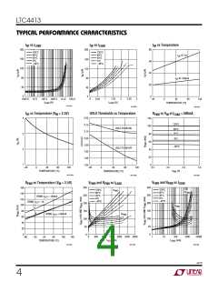
Note 3: Quiescent current increases with diode current, refer to plot of I
QF
vs I
.
OUT
Note 6: Unless otherwise specified, current into a pin is positive and
current out of a pin is negative. All voltages referenced to GND.
4413f
3

 Linear [ Linear ]