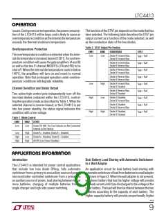
LTC4413
W W
U W
U
W U
ABSOLUTE MAXIMUM RATINGS
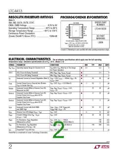
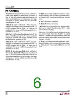
PACKAGE/ORDER INFORMATION
(Note 1)
ORDER PART
NUMBER
INA, INB, OUTA, OUTB, STAT,
TOP VIEW
11
ENBA, ENBB Voltage................................... –0.3V to 6V
Operating Temperature Range ................ – 40°C to 85°C
Storage Temperature Range ................. –65°C to 125°C
Continuous Power Dissipation
INA
ENBA
GND
ENBB
INB
1
2
3
4
5
10 OUTA
9
8
7
6
STAT
NC
LTC4413EDD
NC
OUTB
DD PART
MARKING
(Derate 25mW/°C Above 70°C) ....................... 1500mW
DD PACKAGE
10-LEAD (3mm × 3mm) PLASTIC DFN
LBGN
TJMAX = 125°C, θJA = 40°C/W (4-LAYER PCB)
EXPOSED PAD (PIN 11) IS GND
MUST BE SOLDERED TO PCB
Consult LTC Marketing for parts specified with wider operating temperature ranges.
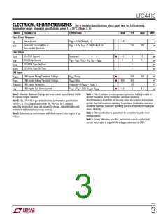
ELECTRICAL CHARACTERISTICS
The ● indicates specifications which apply over the full operating
temperature range, otherwise specifications are at TA = 25°C. (Notes 2, 6)
SYMBOL PARAMETER
CONDITIONS
and/or V Must be in This Range
OUT
MIN
TYP
MAX
UNITS
V , V
Operating Supply Range for Channel A or B
V
●
2.5
5.5
V
IN OUT
IN
for Proper Operation
UVLO
UVLO Turn-On Rising Threshold
Max (V , V , V
, V
)
)
●
●
●
2.4
V
V
INA INB OUTA OUTB
UVLO Turn-Off Falling Threshold
Max (V , V , V
, V
1.7
–1
INA INB OUTA OUTB
I
I
I
I
Quiescent Current in Forward Regulation (Note 3)
V
= 3.6V, I
= 0mA
= –100mA, V = 0V,
25
0.5
22
17
30
2
µA
QF
INA
OUTA
INB
I
OUTB
Current Drawn from or Sourced into IN when
V
= 3.6V, V = 5.5V (Note 6)
OUT
●
µA
µA
µA
LEAK
IN
V
is Greater than V
OUT
IN
Quiescent Current While in Reverse Turn-Off,
Measured via GND
V
V
, V , V
< V
< V
= 5.5V,
= 5.5V
30
23
QRGND
QROUTA
INA INB OUTB
OUTA
OUTA
= 0V
STAT
Quiescent Current While in Reverse Turn-Off,
V
, V , V
INA INB OUTB
●
●
●
Current Drawn from V
Supplies Chip Power
when OUTA
OUTA
I
I
Quiescent Current While in Reverse Turn-Off,
V
, V , V
INA INB OUTA
< V
= 5.5V
and
2
3
µA
µA
QROUTB
QOFF
OUTB
Current Drawn from V
Supplies Chip Power
when OUTB
OUTA
Quiescent Current with Both ENBA
and ENBB High
V
V
= V = 3.6V, V
20
27
INA
INB
ENBA
= 0V
High, V
ENBB
STAT
V
V
Reverse Turn-Off Voltage (V
– V )
V
V
= 3.6V
–5
10
38
mV
mV
RTO
FWD
OUT
IN
IN
IN
Forward Voltage Drop (V – V
)
OUT
= 3.6V
●
28
IN
at I
= –1mA
OUT
R
R
t
On Resistance, R
(Measured as ∆V/∆I)
Regulation
V
V
= 3.6V, I
= 3.6V, I
= –100mA
= –500mA (Note 5)
140
100
mΩ
mΩ
FWD
FWD
IN
IN
OUT
OUT
On Resistance, R Regulation
V
= 3.6V, I
= –1.5A (Note 5)
= –100mA
140
4
200
mΩ
ON
ON
IN
OUT
(Measured as V/I at I = 1A)
PowerPathTM Turn-Off Time
IN
V
= 3.6V, I
µs
OFF
IN
OUT
PowerPath is a trademark of Linear Technology Corporation.
4413f
2

 Linear [ Linear ]