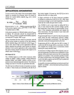
LTC2943
APPLICATIONS INFORMATION
transitioning SDA from low to high while SCL is high. The
bus is then free for another transmission. When the bus
is in use, it stays busy if a repeated START (Sr) is gener-
ated instead of a STOP condition. The repeated START
(Sr) conditions are functionally identical to the START (S).
LTC2943 acknowledges again, increments its address
pointer and latches the second data byte in the following
register, as shown in Figure 6.
S
ADDRESS
1100100
W
A
0
REGISTER
02h
A
0
DATA
F0h
A
0
DATA
01h
A
0
P
0
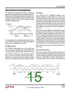
Write Protocol
2943 F06
ThemasterbeginsawriteoperationwithaSTARTcondition
followed by the seven bit slave address 1100100 and the
R/W bit set to zero, as shown in Figure ±. The LTC2943
acknowledges this by pulling SDA low and the master
sends a command byte which indicates which internal
registerthemasteristowrite.TheLTC2943acknowledges
and latches the command byte into its internal register
address pointer. The master delivers the data byte, the
LTC2943 acknowledges once more and latches the data
into the desired register. The transmission is ended when
the master sends a STOP condition. If the master contin-
ues by sending a second data byte instead of a stop, the
Figure 6. Writing F001h to the LTC2943 Accumulated Charge
Register (C, D)
Read Protocol
ThemasterbeginsareadoperationwithaSTARTcondition
followed by the seven bit slave address 1100100 and the
R/W bit set to zero, as shown in Figure 7. The LTC2943
acknowledges and the master sends a command byte
which indicates which internal register the master is to
read. The LTC2943 acknowledges and then latches the
command byte into its internal register address pointer.
The master then sends a repeated START condition fol-
lowed by the same seven bit address with the R/W bit
now set to one. The LTC2943 acknowledges and sends
the contents of the requested register. The transmission
is ended when the master sends a STOP condition. If
the master acknowledges the transmitted data byte, the
LTC2943 increments its address pointer and sends the
contents of the following register as depicted in Figure 8.
S
ADDRESS
1100100
W
A
0
REGISTER
01h
A
0
DATA
FCh
A
0
P
0
2943 F05
FROM MASTER TO SLAVE
FROM SLAVE TO MASTER
A: ACKNOWLEDGE (LOW)
A: NOT ACKNOWLEDGE (HIGH)
S: START CONDITION
P: STOP CONDITION
R: READ BIT (HIGH)
W: WRITE BIT (LOW)
Figure 5. Writing FCh to the LTC2943 Control Register (B)
S
ADDRESS
1100100
W
A
0
REGISTER
00h
A
0
Sr ADDRESS
1100100
R
1
A
0
DATA
01h
A
P
0
1
2943 F07
Figure 7. Reading the LTC2943 Status Register (A)
S
ADDRESS
1100100
W
A
0
REGISTER
08h
A
0
Sr ADDRESS
1100100
R
1
A
0
DATA
F1h
A
0
DATA
24h
A
P
0
1
2943 F08
Figure 8. Reading the LTC2943 Voltage Register (I, J)
2943fa
16
For more information www.linear.com/LTC2943

 Linear [ Linear ]