LTC1410
U U
U
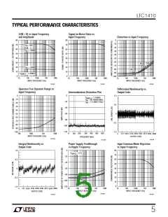
PI FU CTIO S
+A (Pin 1): Positive Analog Input, ±2.5V.
SHDN (Pin 21): Power Shutdown Input. A low logic
level will invoke the Shutdown mode selected by the
NAP/SLP pin.
IN
–A (Pin 2): Negative Analog Input, ±2.5V.
IN
V
REF
(Pin 3): 2.50V Reference Output.
RD (Pin 22): Read Input. This enables the output
drivers when CS is low.
REFCOMP (Pin 4): 4.06V Reference Bypass Pin. By-
pass to AGND with 10µF tantalum in parallel with 0.1µF
ceramic.
CONVST (Pin 23): Conversion Start Signal. This active
low signal starts a conversion on its falling edge.
AGND (Pin 5): Analog Ground.
CS (Pin 24): The Chip Select input must be low for the
ADC to recognize CONVST and RD inputs.
D11 to D4 (Pins 6 to 13): Three-State Data Outputs.
DGND (Pin 14): Digital Ground for Internal Logic. Tie to
AGND.
BUSY (Pin 25): The BUSY output shows the converter
status. It is low when a conversion is in progress. Data
valid on the rising edge of BUSY.
D3 to D0 (Pins 15 to 18): Three-State Data Outputs.
OGND (Pin 19): Digital Ground for Output Drivers. Tie
to AGND.
V (Pin 26): –5V Negative Supply. Bypass to AGND
with 10µF tantalum in parallel 0.1µF ceramic.
SS
NAP/SLP (Pin 20): Power Shutdown Mode. Selects the
mode invoked by the SHDN pin. Low selects Sleep
mode and high selects quick wake-up Nap mode.
DV (Pin 27): 5V Positive Supply. Short to Pin 28.
DD
AV (Pin 28): 5V Positive Supply. Bypass to AGND
DD
with 10µF tantalum in parallel with 0.1µF ceramic.
U
U
W
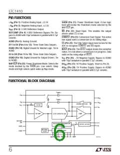
FU CTIO AL BLOCK DIAGRA
C
SAMPLE
+A
IN
AV
DD
C
SAMPLE
–A
IN
DV
DD
2k
ZEROING SWITCHES
V
REF
2.5V REF
REF AMP
V
SS
+
COMP
12-BIT CAPACITIVE DAC
–
REFCOMP
(4V)
12
D11
D0
SUCCESSIVE APPROXIMATION
REGISTER
•
•
•
OUTPUT LATCHES
AGND
DGND
INTERNAL
CLOCK
CONTROL LOGIC
LTC1410 • BD
NAP/SLP SHDN CONVST RD CS BUSY
6

 Linear [ Linear ]