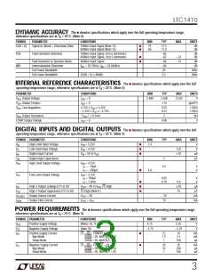
LTC1410
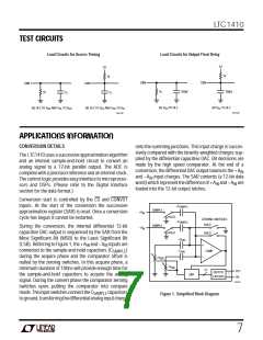
TEST CIRCUITS
Load Circuits for Output Float Delay
Load Circuits for Access Timing
5V
5V
1k
1k
DBN
DBN
DBN
DBN
1k
100pF
100pF
1k
C
L
C
L
(A) V TO Hi-Z
OH
(B) V TO Hi-Z
OL
(A) Hi-Z TO V AND V TO V
(B) Hi-Z TO V AND V TO V
OL OH OL
OH
OL
OH
1410 TC02
1410 TC01
U
W U U
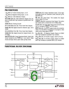
APPLICATIONS INFORMATION
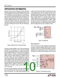
CONVERSION DETAILS
onto the summing junctions. This input charge is succes-
sively compared with the binarily-weighted charges sup-
plied by the differential capacitive DAC. Bit decisions are
made by the high speed comparator. At the end of a
The LTC1410 uses a successive approximation algorithm
and an internal sample-and-hold circuit to convert an
analog signal to a 12-bit parallel output. The ADC is
complete with a precision reference and an internal clock.
The control logic provides easy interface to microproces-
sors and DSPs. (Please refer to the Digital Interface
section for the data format.)
conversion, the differential DAC output balances the +A
IN
and –A input charges. The SAR contents (a 12-bit data
IN
word) which represent the difference of +A and –A are
IN
IN
loaded into the 12-bit output latches.
Conversion start is controlled by the CS and CONVST
inputs. At the start of the conversion the successive
approximation register (SAR) is reset. Once a conversion
cycle has begun it cannot be restarted.
+C
SAMPLE
SAMPLE
SAMPLE
+A
IN
HOLD
HOLD
ZEROING SWITCHES
HOLD
–C
SAMPLE
During the conversion, the internal differential 12-bit
capacitive DAC output is sequenced by the SAR from the
Most Significant Bit (MSB) to the Least Significant Bit
(LSB). Referring to Figure 1, the +A and –A inputs are
–A
IN
HOLD
+C
DAC
+
IN
IN
connected to the sample-and-hold capacitors (CSAMPLE
)
–C
DAC
COMP
during the acquire phase and the comparator offset is
nulled by the zeroing switches. In this acquire phase, a
minimum duration of 100ns will provide enough time for
the sample-and-hold capacitors to acquire the analog
signal. During the convert phase the comparator zeroing
switches open, putting the comparator into compare
mode. The input switches connect the CSAMPLE capacitors
toground, transferringthedifferentialanaloginputcharge
–
+V
DAC
–V
DAC
12
D11
OUTPUT
•
•
•
SAR
LATCHES
D0
1410 F01
Figure 1. Simplified Block Diagram
7

 Linear [ Linear ]