LTC1410
W
U
W W W
U
/O
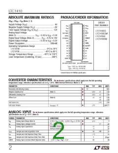
PACKAGE RDER I FOR ATIO
ABSOLUTE AXI U RATI GS
AVDD = DVDD = VDD (Notes 1, 2)
TOP VIEW
ORDER
PART NUMBER
Supply Voltage (VDD)................................................ 6V
+A
1
2
3
4
5
6
7
8
9
28 AV
IN
DD
Negative Supply Voltage (V ) ............................... –6V
SS
–A
IN
27 DV
DD
Total Supply Voltage (VDD to V ) .......................... 12V
SS
V
REF
26
V
SS
LTC1410CG
LTC1410CSW
LTC1410IG
Analog Input Voltage
REFCOMP
AGND
D11(MSB)
D10
25 BUSY
24 CS
(Note 3) .................................. V – 0.3V to VDD + 0.3V
SS
Digital Input Voltage (Note 4) ............ V – 0.3V to 10V
23 CONVST
22 RD
SS
LTC1410ISW
Digital Output Voltage................... – 0.3V to VDD + 0.3V
Power Dissipation............................................. 500mW
Operating Temperature Range
LTC1410C .............................................. 0°C to 70°C
LTC1410I........................................... –40°C to 85°C
Storage Temperature Range ................ –65°C to 150°C
Lead Temperature (Soldering, 10 sec)................. 300°C
D9
21 SHDN
20 NAP/SLP
19 OGND
18 D0
D8
D7 10
D6 11
D5 12
17 D1
D4 13
16 D2
DGND 14
15 D3
G PACKAGE
SW PACKAGE
28-LEAD PLASTIC SSOP 28-LEAD PLASTIC SO WIDE
TJMAX = 110°C, θJA = 90°C/W (SW)
TJMAX = 110°C, θJA = 95°C/W (G)
Consult factory for Military grade parts.
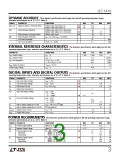
U
CO VERTER
CHARACTERISTICS
The ● denotes specifications which apply over the full operating
temperature range, otherwise specifications are at TA = 25°C. With Internal Reference (Notes 5, 6)
PARAMETER
CONDITIONS
(Note 7)
MIN
TYP
MAX
UNITS
Bits
Resolution (No Missing Codes)
Integral Linearity Error
Differential Linearity Error
Offset Error
●
●
●
12
±0.3
±0.3
±2
±1
±1
LSB
LSB
(Note 8)
±6
±8
LSB
LSB
●
●
Full-Scale Error
±15
LSB
Full-Scale Tempco
I
= 0
±15
ppm/°C
OUT(REF)
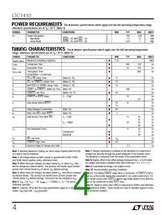
U
U
The ● denotes specifications which apply over the full operating temperature range, otherwise
A ALOG I PUT
specifications are at TA = 25°C. (Note 5)
SYMBOL PARAMETER
CONDITIONS
4.75V ≤ V ≤ 5.25V, –5.25V ≤ V ≤ –4.75V
MIN
TYP
MAX
UNITS
V
V
Analog Input Range (Note 9)
Analog Input Leakage Current
Analog Input Capacitance
●
●
±2.5
IN
DD
SS
I
IN
CS = High
±1
µA
C
IN
Between Conversions
During Conversions
17
5
pF
pF
t
t
t
Sample-and-Hold Acquisition Time
●
50
–1.5
5
100
ns
ns
ACQ
AP
Sample-and-Hold Aperture Delay Time
Sample-and-Hold Aperture Delay Time Jitter
Analog Input Common Mode Rejection Ratio
ps
jitter
RMS
CMRR
–2.5V < (–A = A ) < 2.5V
60
dB
IN
IN
2

 Linear [ Linear ]