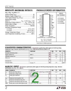
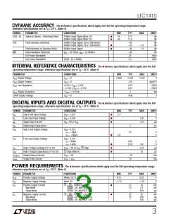
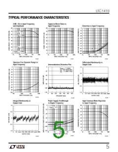
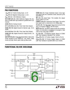
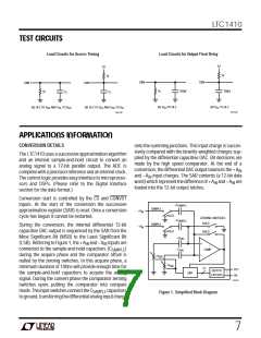
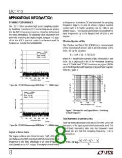
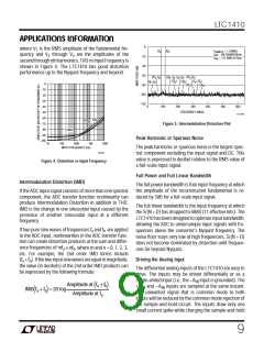
LTC1410
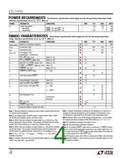
W U
POWER REQUIRE E TS The ● denotes specifications which apply over the full operating temperature range,
otherwise specifications are at TA = 25°C. (Note 5)
SYMBOL
PARAMETER
CONDITIONS
MIN
TYP
MAX
UNITS
P
Power Dissipation
Nap Mode
Sleep Mode
160
7.5
0.01
230
12
1
mW
mW
mW
D
SHDN = 0V, NAP/SLP = 5V
SHDN = 0V, NAP/SLP = 0V
W U
TI I G CHARACTERISTICS The ● denotes specifications which apply over the full operating temperature
range, otherwise specifications are at TA = 25°C. (Note 5)
SYMBOL
PARAMETER
CONDITIONS
MIN
TYP
MAX
UNITS
MHz
ns
f
Maximum Sampling Frequency
Conversion Time
●
●
●
●
1.25
SAMPLE(MAX)
t
t
t
650
50
750
100
800
CONV
Acquisition Time
ns
ACQ
Throughput Time
ns
ACQ+CONV
(Acquisition + Conversion)
t
t
t
t
t
t
CS to RD Setup Time
(Notes 9, 10)
(Notes 9, 10)
(Notes 9, 10)
●
●
●
0
ns
ns
ns
ns
ns
1
2
3
4
5
6
CS↓ to CONVST↓ Setup Time
NAP/SLP↓ to SHDN↓ Setup Time
10
10
SHDN↑ to CONVST↓ Wake-Up Time (Note 10)
200
CONVST Low Time
(Notes 10, 11)
●
●
40
CONVST to BUSY Delay
C = 25pF
L
10
35
ns
ns
50
t
Data Ready Before BUSY↑
20
15
ns
ns
7
●
●
●
t
t
t
Delay Between Conversions
Wait Time RD↓ After BUSY↑
Data Access Time After RD↓
(Note 10)
(Note 10)
40
ns
ns
8
–5
9
C = 25pF
L
15
20
25
35
35
50
ns
ns
ns
ns
10
●
●
C = 100pF
L
t
Bus Relinquish Time
8
20
25
30
ns
ns
ns
11
Commercial
Industrial
●
●
t
t
t
RD Low Time
●
●
t
ns
ns
ns
12
13
14
10
CONVST High Time
40
Aperture Delay of Sample-and-Hold
–1.5
Note 7: Integral nonlinearity is defined as the deviation of a code from a
straight line passing through the actual endpoints of the transfer curve.
The deviation is measured from the center of the quantization band.
Note 1: Absolute Maximum Ratings are those values beyond which the life
of a device may be impaired.
Note 2: All voltage values are with respect to ground with DGND, OGND
Note 8: Bipolar offset is the offset voltage measured from –0.5LSB when
and AGND wired together unless otherwise noted.
the output code flickers between 0000 0000 0000 and 1111 1111 1111.
Note 3: When these pin voltages are taken below V or above V , they
SS
DD
Note 9: Guaranteed by design, not subject to test.
Note 10: Recommended operating conditions.
will be clamped by internal diodes. This product can handle input currents
greater than 100mA below V or above V without latchup.
SS
DD
Note 4: When these pin voltages are taken below V , they will be clamped
by internal diodes. This product can handle input currents greater than
Note 11: The falling CONVST edge starts a conversion. If CONVST returns
high at a critical point during the conversion it can create small errors. For
best results ensure that CONVST returns high either within 425ns after the
start of the conversion or after BUSY rises.
SS
100mA below V without latchup. These pins are not clamped to V
.
SS
DD
Note 5: V = 5V, V = –5V, f
= 1.25MHz, t = t = 5ns unless
r f
DD
SS
SAMPLE
otherwise specified.
Note 12: Signal-to-noise ratio (SNR) is measured at 100kHz and distortion
is measured at 600kHz. These results are used to calculate signal-to-noise
plus distortion (SINAD).
Note 6: Linearity, offset and full-scale specifications apply for a single-
ended +A input with – A grounded.
IN
IN
4

 Linear [ Linear ]