LTC1255
U U
W
U
APPLICATIO S I FOR ATIO
The large output capacitors on many switching regula-
tors, on the other hand, may be able to hold the supply
pinoftheLTC1255above3.5Vsufficientlylongthatthis
extra filtering is not required.
18V
+
C
R
DELAY
100µF
SENSE
0.01µF
0.036Ω
R
DELAY
V
S
100k
DS1
1/2 LTC1255
IN1
1N4148
BecausetheLTC1255ismicropowerinboththestandby
and ON state, the voltage drop across the supply filter
is very small (typically <6mV) and does not signifi-
cantly alter the accuracy of the drain sense threshold
voltage which is typically 100mV.
IRF530
G1
GND
12V
LOAD
LTC1255 • F06
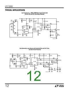
AUTOMOTIVE APPLICATIONS
Reverse Battery Protection
Figure 6. Using a Speed-Up Diode
Current Limited Power Supplies
The LTC1255 can be protected against reverse battery
conditions by connecting a resistor in series with the
groundleadasshowninFigure8.Theresistorlimitsthe
supply current to less than 120mA with –12V applied.
Since the LTC1255 draws very little current while in
normal operation, the drop across the ground resistor
is minimal. The 5V µP (or controlling logic) is protected
by the 10k resistors in series with the input.
The LTC1255 requires at least 3.5V at the supply pin to
ensure proper operation. It is therefore necessary that
the supply to the LTC1255 be held higher than 3.5V at
all times, even when the output of the switch is short
circuited to ground. The output voltage of a current
limited regulator may drop very quickly during short
circuit and pull the supply pin of the LTC1255 below
3.5V before the shutdown circuitry has had time to
respond and remove drive from the gate of the power
MOSFET. A supply filter should be added as shown in
Figure 7 which holds the supply pin of the LTC1255
high long enough for the overcurrent shutdown cir-
cuitry to respond and fully discharge the gate.
14V
+
5V
28V
10µF
R
SENSE
0.036Ω
V
S
DS1
1/2 LTC1255
IN1
µp OR
CONTROL
LOGIC
10k
MTP12N06E
G1
Linear regulators with small output capacitors are the
most difficult to protect as they can “switch” from a
voltage mode to a current limited mode very quickly.
GND
12V
LOAD
100Ω
LTC1255 • F08
12V/2A
15V
REGULATOR
+
+
10Ω*
0.01µF
Figure 8. Reverse Battery Protection
10µF
10µF
R
SENSE
0.1Ω
+
V
S
100k
47µF*
Transient Overvoltage Protection
DS1
1/2 LTC1255
IN1
A common scheme used to limit overvoltage transients
on a 14V nominal automotive power bus is to clamp the
supply to the module containing the high-side MOSFET
switches with a large transient suppressor diode, D1 in
Figure 9. This diode limits the supply voltage to 40V
underworsecaseconditions. TheLTC1255isdesigned
to survive short (10ms) 40V transients and return to
normal operation after the transient has passed.
1N4148
MTP12N06E
G1
GND
12V
SHORT
CIRCUIT
*SUPPLY FILTER COMPONENT
LTC1255 • F07
Figure 7. Supply Filter for Current Limited Supplies
9

 Linear [ Linear ]