LTC1255
U U
W
U
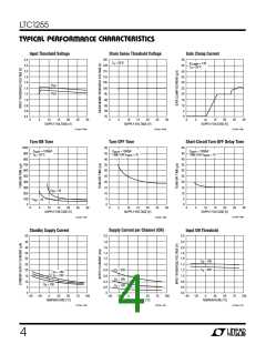
APPLICATIO S I FOR ATIO
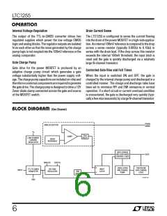
MOSFET AND LOAD PROTECTION
Large inductive loads (>0.1mH) may require diodes con-
nected directly across the inductor to safely divert the
stored energy to ground. Many inductive loads have these
diodes included. Ifnot, adiode ofthe propercurrent rating
should be connected across the load, as shown in
Figure 2, to safely divert the stored energy.
The LTC1255 protects the power MOSFET switch by
removing drive from the gate as soon as an overcurrent
condition is detected. Resistiveandinductiveloadscanbe
protected with no external time delay in series with the
drain sense pin. Lamp loads, however, require that the
overcurrentprotectionbedelayedlongenoughtostartthe
lampbutshortenoughtoensurethesafetyoftheMOSFET.
12V
+
R
100µF
SENSE
0.036Ω
V
S
DS1
1/2 LTC1255
IN1
Resistive Loads
Loads that are primarily resistive should be protected with
asshortadelayaspossibletominimizetheamountoftime
that the MOSFET is subjected to an overload condition.
The drain sense circuitry has a built-in delay of approxi-
mately 10µs to eliminate false triggering by power supply
or load transient conditions. This delay is sufficient to
“mask” short load current transients and the starting of a
small capacitor (<1µF) in parallel with the load. The drain
sense pin can therefore be connected directly to the drain
current sense resistor as shown in Figure 1.
IRFZ24
G1
GND
12V
12V, 1A
SOLENOID
1N5400
LTC1255 • F02
Figure 2. Protecting Inductive Loads
18V
Capacitive Loads
+
R
10µF
SENSE
0.036Ω
Large capacitive loads, such as complex electrical sys-
tems with large bypass capacitors, should be powered
using the circuit shown in Figure 3. The gate drive to the
power MOSFET is passed through an RC delay network,
R1 and C1, which greatly reduces the turn-on ramp rate of
the switch. And since the MOSFET source voltage follows
the gate voltage, the load is powered smoothly and slowly
from ground. This dramatically reduces the startup cur-
rent flowing into the supply capacitor(s) which, in turn,
reduces supply transients and allows for slower activation
V
S
DS1
1/2 LTC1255
IN1
IRFZ24
G1
GND
12V
C
LOAD
R
LOAD
18Ω
≤ 1µF
LTC1255 • F01
Figure 1. Protecting Resistive Loads
15V
+
C
R
DELAY
470µF
SENSE
R
DELAY
0.01µF
0.036Ω
V
S
100k
Inductive Loads
DS1
1/2 LTC1255
IN1
D1
1N4148
Loads that are primarily inductive, such as relays, sole-
noids and stepper motor windings, should be protected
with as short a delay as possible to minimize the amount
of time that the MOSFET is subjected to an overload
condition. The built-in 10µs delay will ensure that the
overcurrent protection is not false triggered by a supply or
load transient. No external delay components are required
as shown in Figure 2.
MTP3055E
G1
GND
R1
100k
R2
100k
12V
+
C1
0.33µF
C
LOAD
100µF
LTC1255 • F03
Figure 3. Powering Large Capacitive Loads
7

 Linear [ Linear ]