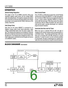
LTC1255
APPLICATIO S I FOR ATIO
of sensitive electrical loads. (Resistor R2, and the diode
D1, provide a direct path for the LTC1255 protection
circuitry to quickly discharge the gate in the event of an
overcurrent condition.)
U U
W
U
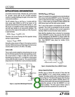
Selecting RDELAY and CDELAY
Figure5isagraphofnormalizedovercurrentshutdown
time versus normalized MOSFET current. This graph is
used to select the two delay components, R
and
DELAY
The RC network, RDELAY and CDELAY, in series with the
drain sense input should be set to trip based on the
expected characteristics of the load after startup, i.e., with
this circuit, it is possible to power a large capacitive load
and still react quickly to an overcurrent condition. The
ramp rate at the output of the switch as it lifts off ground
is approximately:
C
, which make up a simple RC delay between the
DELAY
drain sense input and the drain sense resistor.
The Y axis of the graph is normalized to one RC time
constant. The X axis is normalized to the set current.
(The set current is defined as the current required to
develop 100mV across the drain sense resistor.)
Note that the shutdown time is shorter for increasing
levels of MOSFET current. This ensures that the total
energy dissipated by the MOSFET is always within the
boundsestablishedbythemanufacturerforsafeopera-
tion. (See MOSFET data sheet for further S.O.A.
information.)
dV/dt = (VGATE – VTH)/(R1 × C1)
Therefore, the current flowing into the capacitor during
startup is approximately:
ISTARTUP = CLOAD × dV/dt
Using the values shown in Figure 3, the startup current is
lessthan100mAanddoesnotfalsetriggerthedrainsense
circuitry which is set at 2.7A with a 1ms delay.
10
1
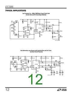
Lamp Loads
The in-rush current created by a lamp during turn-on can
be 10 to 20 times greater than the rated operating current.
The circuit shown in Figure 4 shifts the current limit
threshold up by a factor of 11:1 (to 30A) for a short period
of time while the bulb is turned on. The current limit then
dropsdownto2.7Aafterthein-rushcurrenthassubsided.
0.1
0.01
0.1
1
10
100
NORMALIZED MOSFET CURRENT (1 = SET CURRENT)
LTC1255 • F05
12V
+
10k
470µF
R
SENSE
0.036Ω
Figure 5. Normalized Delay Time vs MOSFET Current
100k
V
S
DS1
1/2 LTC1255
IN1
Using a Speed-Up Diode
VN2222LL
0.1µF
Another way to reduce the amount of time that the
power MOSFET is in a short-circuit condition is to
“bypass” the delay resistor with a small signal diode as
shown in Figure 6. The diode will engage when the drop
across the drain sense resistor exceeds about 0.7V,
providingadirectpathtothesensepinanddramatically
reducing the amount of time the MOSFET is in an
overload condition. The drain sense resistor value is
selected to limit the maximum DC current to 4A.
MTP3055EL
G1
GND
1M
9.1V
12V/1A
BULB
LTC1255 • F04
Figure 4. Lamp Driver With Delayed Protection
8

 Linear [ Linear ]