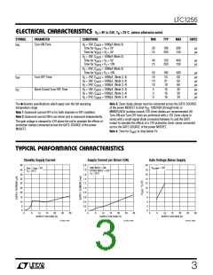
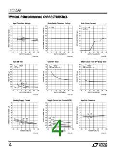
LTC1255
U
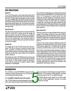
OPERATIO
Internal Voltage Regulation
Drain Current Sense
The output of the TTL-to-CMOS converter drives two
regulated supplies which power the low voltage CMOS
logicandanalogblocks.Theregulatoroutputsareisolated
from each other so that the noise generated by the charge
pump logic is not coupled into the 100mV reference or the
analog comparator.
The LTC1255 is configured to sense the current flowing
into the drain of the power MOSFET in a high-side applica-
tion. An internal 100mV reference is compared to the drop
across a sense resistor (typically 0.002Ω to 0.10Ω) in
series with the drain lead. If the drop across this resistor
exceeds the internal 100mV threshold, the input latch is
reset and the gate is quickly discharged via a relatively
large N-channel transistor.
Gate Charge Pump
Gate drive for the power MOSFET is produced by an
adaptive charge pump circuit which generates a gate
voltage substantially higher than the power supply volt-
age.Thechargepumpcapacitorsareincludedon-chipand
thereforenoexternalcomponentsarerequiredtogenerate
the gate drive. The charge pump is designed to drive a 12V
Zener diode clamp connected across the gate and source
of the MOSFET switch.
Controlled Gate Rise and Fall Times
When the input is switched ON and OFF, the gate is
charged by the internal charge pump and discharged in a
controlled manner. The charge and discharge rates have
been set to minimize RFI and EMI emissions in normal
operation. If a short circuit or current overload condition
is encountered, the gate is discharged very quickly (typi-
cally a few microseconds) by a large N-channel transistor.
W
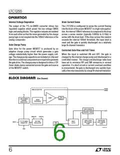
BLOCK DIAGRA
(One Channel)
DRAIN
SENSE
ANALOG SECTION
V
S
10µs
DELAY
COMP
LOW STANDBY
CURRENT
REGULATOR
100mV
REFERENCE
GATE CHARGE
AND DISCHARGE
CONTROL LOGIC
GATE
ANALOG
DIGITAL
R
S
OSCILLATOR
AND CHARGE
PUMP
FAST/SLOW
GATE CHARGE
LOGIC
TTL-TO-CMOS
CONVERTER
VOLTAGE
REGULATOR
INPUT
LATCH
INPUT
ONE
SHOT
LTC1255 • BD
GND
6

 Linear [ Linear ]