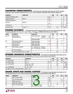
LTC1400
U U
W U
APPLICATIO S I FOR ATIO
Conversion Details
Dynamic Performance
TheLTC1400hasexcellenthighspeedsamplingcapability.
FFT (Fast Fourier Transform) test techniques are used to
test the ADC’s frequency response, distortion and noise
at the rated throughput. By applying a low distortion
sine wave and analyzing the digital output using an FFT
algorithm, the ADC’s spectral content can be examined for
frequencies outside the fundamental. Figure 2a shows a
typical LTC1400 FFT plot.
The LTC1400 uses a successive approximation algorithm
and an internal sample-and-hold circuit to convert an
analog signal to a 12-bit serial output based on a preci-
sion internal reference. The control logic provides easy
interface to microprocessors and DSPs through 3-wire
connections.
A rising edge on the CONV input starts a conversion. At
the start of a conversion the successive approximation
register(SAR)isreset. Onceaconversioncyclehasbegun
it cannot be restarted.
Signal-to-Noise Ratio
The signal-to-noise plus distortion ratio [S/(N + D)] is the
ratiobetweentheRMSamplitudeofthefundamentalinput
frequency to the RMS amplitude of all other frequency
components at the A/D output. The output is band limited
to frequencies from DC to half the sampling frequency.
Figure 2a shows a typical spectral content with a 400kHz
sampling rate and a 100kHz input. The dynamic perfor-
mance is excellent for input frequencies up to the Nyquist
limit of 200kHz as shown in Figure 2b.
During conversion, the internal 12-bit capacitive DAC
output is sequenced by the SAR from the most significant
bit (MSB) to the least significant bit (LSB). Referring to
Figure 1, the A input connects to the sample-and-hold
IN
capacitor during the acquired phase and the comparator
offset is nulled by the feedback switch. In this acquire
phase, it typically takes 200ns for the sample-and-hold
capacitor to acquire the analog signal. During the convert
phase, the comparator feedback switch opens, putting the
comparator into the compare mode. The input switches
0
f
f
= 400kHz
SAMPLE
IN
–10
–20
= 94.824kHz
connect C
to ground, injecting the analog input
SINAD = 72.5dB
THD = –82dB
SAMPLE
–30
charge onto the summing junction. This input charge is
successively compared with the binary-weighted charges
supplied by the capacitive DAC. Bit decisions are made by
the high speed comparator. At the end of a conversion,
–40
–50
–60
–70
–80
the DAC output balances the A input charge. The SAR
IN
–90
contents (a 12-bit data word) which represent the input
–100
–110
–120
voltage, are output through the serial pin D
.
OUT
0
20 40 60 80 100 120 140 160 180 200
FREQUENCY (kHz)
SAMPLE
S1
1400 F02a
C
SAMPLE
DAC
Figure 2a. LTC1400 Nonaveraged, 4096 Point FFT
Plot with 100kHz Input Frequency in Bipolar Mode
SAMPLE
HOLD
–
+
A
IN
COMP
Effective Number of Bits
C
V
DAC
The effective number of bits (ENOBs) is a measurement
of the effective resolution of an ADC and is directly related
to the S/(N + D) by the equation:
S
A
R
DAC
D
OUT
S / N+D –1.76
(
)
1400 F01
N=
6.02
Figure 1. A Input
IN
1400fa
7

 Linear [ Linear ]