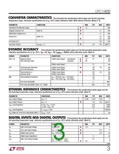
LTC1400
U U
U
PI FU CTIO S
V
(Pin 1): Positive Supply, 5V. Bypass to GND (10μF
CLK (Pin 6): Clock. This clock synchronizes the serial data
transfer. A minimum CLK pulse of 50ns will cause the ADC
to wake up from Nap or Sleep mode.
CC
tantalum in parallel with 0.1μF ceramic).
A (Pin2):AnalogInput.0Vto4.096V(Unipolar),±2.048V
IN
(Bipolar).
CONV (Pin 7): Conversion Start Signal. This active high
signal starts a conversion on its rising edge. Keeping CLK
low and pulsing CONV two/four times will put the ADC
into Nap/Sleep mode.
V
(Pin 3): 2.42V Reference Output. Bypass to GND
REF
(10μF tantalum in parallel with 0.1μF ceramic).
GND (Pin 4): Ground. GND should be tied directly to an
analog ground plane.
V
(Pin 8): Negative Supply. –5V for bipolar operation.
SS
Bypass to GND with 0.1μF ceramic. V should be tied to
SS
D
(Pin 5): The A/D conversion result is shifted out
GND for unipolar operation.
OUT
from this pin.
U
U
W
FU CTIO AL BLOCK DIAGRA
C
ZEROING SWITCH
SAMPLE
V
A
CC
IN
GND
V
SS
V
REF
2.42V REF
12-BIT CAPACITIVE DAC
COMP
CLK
12
CONTROL
LOGIC
CONV
SUCCESSIVE APPROXIMATION
REGISTER/PARALLEL TO
SERIAL CONVERTER
D
OUT
1400 BD01
TEST CIRCUITS
5V
3k
D
OUT
D
OUT
3k
C
LOAD
C
LOAD
Hi-Z TO V
OH
Hi-Z TO V
OL
V
OL
OH
TO V
OH
V
OH
OL
TO V
OL
V
TO Hi-Z
V
TO Hi-Z
1400 TC01
1400fa
6

 Linear [ Linear ]