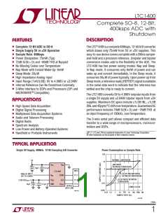
LTC1400
U
U
DIGITAL I PUTS A D DIGITAL OUTPUTS
The
●
denotes the specifications which apply over the
full operating temperature range, otherwise specifications are at T = 25°C unless otherwise noted. (Note 5)
A
SYMBOL
PARAMETER
CONDITIONS
MIN
TYP
MAX
UNITS
V
Low Level Output Voltage
V
V
= 4.75V, I = 160μA
0.05
0.10
V
V
OL
CC
CC
O
●
●
= 4.75V, I = 1.6mA
0.4
O
I
OZ
Hi-Z Output Leakage D
V
OUT
= 0V to V
±10
μA
pF
OUT
CC
C
Hi-Z Output Capacitance D
Output Source Current
Output Sink Current
(Note 7)
15
–10
10
OZ
OUT
I
I
V
V
= 0V
mA
mA
SOURCE
OUT
= V
SINWK U
OUT
CC
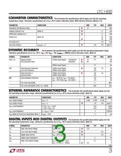
TI I G CHARACTERISTICS
The
●
denotes the specifications which apply over the full operating temperature
range, otherwise specifications are at T = 25°C unless otherwise noted. (Note 5)
A
SYMBOL
PARAMETER
CONDITIONS
MIN
TYP
MAX
UNITS
kHz
●
●
f
t
t
Maximum Sampling Frequency
Conversion Time
(Note 6)
400
SAMPLE(MAX)
CONV
f
= 6.4MHz
2.1
μs
CLK
●
●
Acquisition Time
(Unipolar Mode)
(Bipolar Mode V = –5V)
(Note 7)
230
200
300
270
ns
ns
ACQ
SS
●
●
f
t
t
t
t
t
t
t
t
t
CLK Frequency
0.1
50
6.4
MHz
ns
ns
ns
ns
ns
ns
ns
ns
CLK
CLK Pulse Width
(Notes 7, 12)
(Note 7)
CLK
Time to Wake Up from Nap Mode
CLK Pulse Width to Return to Active Mode
CONV↑ to CLK↑ Setup Time
350
WK(NAP)
●
●
●
●
50
80
0
1
2
3
4
5
6
7
CONV↑ After Leading CLK↑
CONV Pulse Width
(Note 11)
50
Time from CLK↑ to Sample Mode
Aperture Delay of Sample-and-Hold
Minimum Delay Between Conversion (Unipolar Mode)
(Note 7)
80
45
●
Jitter < 50ps (Note 7)
65
●
●
265
235
385
355
ns
ns
(Bipolar Mode V = –5V)
SS
●
●
●
●
t
t
t
t
Delay Time, CLK↑ to D
Delay Time, CLK↑ to D
Valid
Hi-Z
C
C
C
= 20pF
= 20pF
= 20pF
40
40
25
80
80
ns
ns
ns
ns
8
OUT
LOAD
LOAD
LOAD
9
OUT
Time from Previous Data Remains Valid After CLK↑
Minimum Time between Nap/Sleep Request to Wake Up Request
14
50
10
11
(Notes 7, 12)
Note 1: Stresses beyond those listed under Absolute Maximum Ratings
may cause permanent damage to the device. Exposure to any Absolute
Maximum Rating condition for extended periods may affect device
reliability and lifetime.
Note 7: Guaranteed by design, not subject to test.
Note 8: Linearity, offset and full-scale specifications apply for unipolar and
bipolar modes.
Note 9: Integral nonlinearity is defined as the deviation of a code from a
straight line passing through the actual endpoints of the transfer curve.
The deviation is measured from the center of the quantization band.
Note 10: Bipolar offset is the offset voltage measured from –0.5LSB when
the output code flickers between 0000 0000 0000 and 1111 1111 1111.
Note 11: The rising edge of CONV starts a conversion. If CONV returns
low at a bit decision point during the conversion, it can create small errors.
For best performance ensure that CONV returns low either within 120ns
after conversion starts (i.e., before the first bit decision) or after the 14
clock cycle. (Figure 13 Timing Diagram).
Note 2: All voltage values are with respect to GND.
Note 3: When these pin voltages are taken below V (ground for unipolar
SS
mode) or above V , they will be clamped by internal diodes. This product
CC
can handle input currents greater than 40mA below V (ground for
SS
unipolar mode) or above V without latch-up.
CC
Note 4: When these pin voltages are taken below V (ground for unipolar
SS
mode), they will be clamped by internal diodes. This product can handle
input currents greater than 40mA below V (ground for unipolar mode)
SS
without latch-up. These pins are not clamped to V
.
CC
Note 5: V = 5V, f
= 400kHz, t = t = 5ns unless otherwise
r f
CC
SAMPLE
Note 12: If this timing specification is not met, the device may not respond
specified.
to a request for a conversion. To recover from this condition a NAP
Note 6: Recommended operating conditions.
request is required.
1400fa
4

 Linear [ Linear ]