LTC1400
U
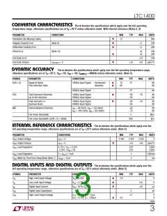
CO VERTER CHARACTERISTICS
The
●
denotes the specifications which apply over the full operating
temperature range, otherwise specifications are at T = 25°C unless otherwise noted. With internal reference (Notes 5, 8)
A
PARAMETER
CONDITIONS
MIN
TYP
MAX
UNITS
Bits
●
●
●
Resolution (No Missing Codes)
Integral Linearity Error
Differential Linearity Error
Offset Error
12
(Note 9)
±1
±1
LSB
LSB
(Note 10)
±6
±8
LSB
LSB
●
●
Full-Scale Error
Full-Scale Tempco
U W
±15
±45
LSB
I
= 0
±10
ppm/°C
OUT(REF)
DY A IC ACCURACY
The
●
denotes the specifications which apply over the full operating temperature range,
= 400kHz unless otherwise noted. (Note 5)
otherwise specifications are at T = 25°C. V = 5V, V = –5V, f
SAMPLE
A
CC
SS
SYMBOL
PARAMETER
CONDITIONS
MIN
TYP
MAX
UNITS
●
●
S/(N + D)
Signal-to-Noise
Plus Distortion Ratio
100kHz Input Signal
Commercial
Industrial
70
69
72
dB
dB
200kHz Input Signal
72
dB
●
●
THD
Total Harmonic Distortion
Up to 5th Harmonic
100kHz Input Signal
200kHz Input Signal
–82
–80
–76
–76
dB
dB
Peak Harmonic or
Spurious Noise
100kHz Input Signal
200kHz Input Signal
–84
–82
dB
dB
IMD
Intermodulation Distortion
f
f
= 99.51kHz, f = 102.44kHz
–82
–70
dB
dB
IN1
IN1
IN2
= 199.12kHz, f = 202.05kHz
IN2
Full Power Bandwidth
4
MHz
kHz
U U Full Linear BandwidtUh (S/(N + D) ≥ 68dB)
I TER AL REFERE CE CHARACTERISTICS
900
The
●
denotes the specifications which apply over the
full operating temperature range, otherwise specifications are at T = 25°C unless otherwise noted. (Note 5)
A
PARAMETER
CONDITIONS
MIN
TYP
2.420
±10
MAX
2.440
±45
UNITS
V
V
V
V
Output Voltage
Output Tempco
Load Regulation
I
I
= 0
= 0
2.400
REF
REF
REF
OUT
OUT
●
ppm/°C
4.75V ≤ V ≤ 5.25V
0.01
0.01
LSB/V
LSB/V
CC
–5.25V ≤ V ≤ 0V
SS
V
V
Load Regulation
0 ≤ |I | ≤ 1mA
2
4
LSB/mA
ms
REF
REF
OUT
Wake-Up Time from Sleep Mode (Note 7)
C
= 10μF
VREF
U
U
DIGITAL I PUTS A D DIGITAL OUTPUTS
The
●
denotes the specifications which apply over the
full operating temperature range, otherwise specifications are at T = 25°C unless otherwise noted. (Note 5)
A
SYMBOL
PARAMETER
CONDITIONS
MIN
TYP
MAX
UNITS
V
●
●
●
V
V
High Level Input Voltage
Low Level Input Voltage
Digital Input Current
Digital Input Capacitance
High Level Output Voltage
V
CC
V
CC
V
IN
= 5.25V
= 4.75V
= 0V to V
2.0
IH
IL
0.8
V
I
IN
±10
μA
pF
CC
C
V
5
IN
V
CC
V
CC
= 4.75V, I = –10μA
= 4.75V, I = –200μA
4.7
V
V
OH
O
O
●
4.0
1400fa
3

 Linear [ Linear ]