LTC1400
W W W U
U
W
U
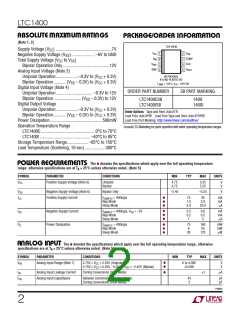
ABSOLUTE AXI U RATI GS
PACKAGE/ORDER I FOR ATIO
(Note 1, 2)
TOP VIEW
Supply Voltage (V ) ..................................................7V
CC
V
V
SS
1
2
3
4
8
7
6
5
CC
Negative Supply Voltage (V )..................... –6V to GND
SS
A
CONV
CLK
IN
Total Supply Voltage (V to V )
CC
SS
V
REF
Bipolar Operation Only..........................................12V
Analog Input Voltage (Note 3)
GND
D
OUT
S8 PACKAGE
8-LEAD PLASTIC SO
Unipolar Operation....................–0.3V to (V + 0.3V)
CC
Bipolar Operation........... (V – 0.3V) to (V + 0.3V)
SS
CC
T
= 150°C, θ = 130°C/W
JA
JMAX
Digital Input Voltage (Note 4)
ORDER PART NUMBER
S8 PART MARKING
Unipolar Operation................................. –0.3V to 12V
Bipolar Operation.........................(V – 0.3V) to 12V
SS
LTC1400CS8
LTC1400IS8
1400
1400I
Digital Output Voltage
Unipolar Operation....................–0.3V to (V + 0.3V)
CC
Order Options Tape and Reel: Add #TR
Bipolar Operation........... (V – 0.3V) to (V + 0.3V)
SS
CC
Lead Free: Add #PBF Lead Free Tape and Reel: Add #TRPBF
Lead Free Part Marking: http://www.linear.com/leadfree/
Power Dissipation.............................................. 500mW
Operation Temperature Range
Consult LTC Marketing for parts specified with wider operating temperature ranges.
LTC1400C ................................................ 0°C to 70°C
LTC1400I ............................................. –40°C to 85°C
Storage Temperature Range................... –65°C to 150°C
Lead Temperature (Soldering, 10 sec) .................. 300°C
W U
POWER REQUIRE E TS The
●
denotes the specifications which apply over the full operating temperature
range, otherwise specifications are at T = 25°C unless otherwise noted. (Note 5)
A
SYMBOL
PARAMETER
CONDITIONS
MIN
TYP
MAX
UNITS
V
Positive Supply Voltage (Note 6)
Unipolar
Bipolar
4.75
4.75
5.25
5.25
V
V
CC
V
Negative Supply Voltage (Note 6)
Positive Supply Current
Bipolar Only
–2.45
–5.25
V
SS
●
●
●
I
I
f
= 400ksps
SAMPLE
15
1.0
5.0
30
3.0
20.0
mA
mA
μA
CC
Nap Mode
Sleep Mode
●
●
●
Negative Supply Current
Power Dissipation
f
= 400ksps, V = –5V
0.3
0.2
1
0.6
0.5
5
mA
mA
μA
SS
SAMPLE
SS
Nap Mode
Sleep Mode
●
●
●
P
f
= 400ksps
SAMPLE
75
6
30
160
20
125
mW
mW
μW
D
Nap Mode
Sleep Mode
U
U
A ALOG I PUT The
●
denotes the specifications which apply over the full operating temperature range, otherwise
specifications are at T = 25°C unless otherwise noted. (Note 5)
A
SYMBOL
PARAMETER
CONDITIONS
4.75V ≤ V ≤ 5.25V (Unipolar)
MIN
TYP
MAX
UNITS
●
●
V
Analog Input Range (Note 7)
0 to 4.096
±2.048
V
V
IN
CC
4.75V ≤ V ≤ 5.25V, –5.25V ≤ V ≤ –2.45V (Bipolar)
CC
SS
●
I
Analog Input Leakage Current
Analog Input Capacitance
During Conversions (Hold Mode)
±1
μA
IN
C
Between Conversions (Sample Mode)
During Conversions (Hold Mode)
45
5
pF
pF
IN
1400fa
2

 Linear [ Linear ]