LTC3787
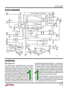
OPERATION
multiple LTC3787s can be configured for 2-, 3-, 4- , 6- and
12-phase operation.
Power Good
The PGOOD pin is connected to an open drain of an
internal N-channel MOSFET. The MOSFET turns on and
pulls the PGOOD pin low when the VFB pin voltage is not
within 10% of the 1.2V reference voltage. The PGOOD
pin is also pulled low when the corresponding RUN pin
is low (shut down). When the VFB pin voltage is within
the 10% requirement, the MOSFET is turned off and the
pin is allowed to be pulled up by an external resistor to a
source of up to 6V (abs max).
Table ±.
V
CONTROLLER 2 PHASE (°C)
CLKOUT PHASE (°C)
PHASMD
GND
180
180
240
60
90
Floating
INTV
120
CC
CLKOUT is disabled when the controller is in shutdown
or in sleep mode.
Operation When V > Regulated V
IN
OUT
Operation at Low SENSE Pin Common Mode Voltage
WhenV risesabovetheregulatedV voltage,theboost
IN
OUT
ThecurrentcomparatorintheLTC3787ispowereddirectly
controller can behave differently depending on the mode,
+
from the SENSE pin. This enables the common mode
inductor current and V voltage. In forced continuous
+
–
IN
voltage of the SENSE and SENSE pins to operate at as
lowas2.5V, whichisbelowtheUVLOthreshold. Thefigure
on the first page shows a typical application in which the
mode, the loop works to keep the top MOSFET on con-
tinuously once V rises above V . The internal charge
IN
OUT
pump delivers current to the boost capacitor to maintain
a sufficiently high TG voltage. The amount of current the
charge pump can deliver is characterized by two curves
in the Typical Performance Characteristics section.
controller’s VBIAS is powered from V
while the V
OUT
IN
+
supply can go as low as 2.5V. If the voltage on SENSE
drops below 2.5V, the SS pin will be held low. When the
SENSE voltage returns to the normal operating range, the
SS pin will be released, initiating a new soft-start cycle.
In pulse-skipping mode, if V is between 100% and
IN
110% of the regulated V
voltage, TG turns on if the
OUT
BOOST Supply Refresh and Internal Charge Pump
inductor current rises above a certain threshold and turns
off if the inductor current falls below this threshold. This
threshold current is set to approximately 6%, 4% or
3% of the maximum ILIM current when the ILIM pin is
Each top MOSFET driver is biased from the floating
bootstrap capacitor, C , which normally recharges during
B
each cycle through an external diode when the bottom
MOSFET turns on. There are two considerations for keep-
ing the BOOST supply at the required bias level. During
start-up, if the bottom MOSFET is not turned on within
100μs after UVLO goes low, the bottom MOSFET will be
forced to turn on for ~400ns. This forced refresh gener-
ates enough BOOST-SW voltage to allow the top MOSFET
ready to be fully enhanced instead of waiting for the initial
few cycles to charge up. There is also an internal charge
pump that keeps the required bias on BOOST. The charge
pump always operates in both forced continuous mode
and pulse-skipping mode. In Burst Mode operation, the
charge pump is turned off during sleep and enabled when
the chip wakes up. The internal charge pump can normally
supply a charging current of 55μA.
grounded, floating or tied to INTV , respectively. If the
CC
controller is programmed to Burst Mode operation under
this same V window, then TG remains off regardless of
IN
the inductor current.
If V rises above 110% of the regulated V
voltage in
IN
OUT
any mode, the controller turns on TG regardless of the
inductor current. In Burst Mode operation, however, the
internal charge pump turns off if the chip is asleep. With
the charge pump off, there would be nothing to prevent
the boost capacitor from discharging, resulting in an
insufficient TG voltage needed to keep the top MOSFET
completely on. To prevent excessive power dissipation
across the body diode of the top MOSFET in this situation,
the chip can be switched over to forced continuous mode
to enable the charge pump or a Schottky diode can also
be placed in parallel to the top MOSFET.
3787fc
14

 Linear Systems [ Linear Systems ]