LTC3787
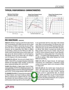
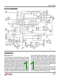
BLOCK DIAGRAM
INTV
CC
PHASMD
CLKOUT
DUPLICATE FOR SECOND CONTROLLER CHANNEL
S
D
BOOST
TG
B
Q
R
C
B
SHDN
SWITCHING
LOGIC
V
OUT
SW
AND
C
OUT
20ꢀA
CHARGE
PUMP
INTV
CC
FREQ
CLK2
CLK1
BG
VCO
PFD
+
–
0.425V
–
SLEEP
PGND
L
+
I
I
REV
CMP
+
+
–
+
–
–
–
2mV
SENSE
SENSE
2.8V
0.7V
PLLIN/
MODE
R
SENSE
+
SLOPE COMP
SENS LO
SYNC
DET
V
IN
C
+
IN
100k
–
2.5V
ILIM
VFB
CURRENT
LIMIT
+
–
–
1.2V
SS
EA
VBIAS
SHDN
+
–
EXTV
CC
OV
1.32V
C
C
ITH
0.5ꢀA/
4.5ꢀA
5.4V
LDO
5.4V
LDO
+
–
R
C
C
PGOOD
EN
EN
C2
+
–
1.32V
10ꢀA
SS
3.8V
11V
+
VFB
+
–
–
4.8V
INTV
SENS
LO
SGND
CC
SHDN
RUN
1.08V
C
SS
3787 BD
OPERATION
Main Control Loop
connected across the output voltage, V , to ground), to
OUT
theinternal1.200Vreferencevoltage. Inaboostconverter,
the required inductor current is determined by the load
The LTC3787 uses a constant-frequency, current mode
step-up architecture with the two controller channels
operating out of phase. During normal operation, each
external bottom MOSFET is turned on when the clock for
that channel sets the RS latch, and is turned off when the
main current comparator, ICMP, resets the RS latch. The
peak inductor current at which ICMP trips and resets the
latch is controlled by the voltage on the ITH pin, which is
the output of the error amplifier EA. The error amplifier
compares the output voltage feedback signal at the VFB
pin (which is generated with an external resistor divider
current, V and V . When the load current increases,
IN
OUT
it causes a slight decrease in VFB relative to the reference,
which causes the EA to increase the ITH voltage until the
averageinductorcurrentineachchannelmatchesthenew
requirement based on the new load current.
After the bottom MOSFET is turned off each cycle, the
top MOSFET is turned on until either the inductor current
starts to reverse, as indicated by the current comparator,
IR, or the beginning of the next clock cycle.
3787fc
11

 Linear Systems [ Linear Systems ]