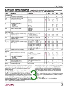
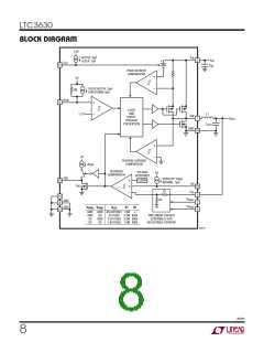
LTC3630
PIN FUNCTIONS
SW (Pin 1): Switch Node Connection to Inductor. This
pin connects to the drains of the internal power MOSFET
switches.
SS (Pin 10): Soft-Start Control Input. A capacitor to
ground at this pin sets the output voltage ramp time. A
50ꢀA current initially charges the soft-start capacitor until
switching begins, at which time the current is reduced to
its nominal value of 5ꢀA. The output voltage ramp time
from zero to its regulated value is 1ms for every 16.5nF
of capacitance from SS to GND. If left floating, the ramp
time defaults to an internal 0.8ms soft-start.
NC (Pins 2, 4, 13, 15 DHC Package Only): No Internal
Connection. Leave these pins open.
V
(Pin 3): Main Input Supply Pin. A ceramic bypass
IN
capacitor should be tied between this pin and GND.
RUN (Pin 5): Run Control Input. A voltage on this pin
above 1.21V enables normal operation. Forcing this pin
below 0.7V shuts down the LTC3630, reducing quiescent
current to approximately 5ꢀA. Optionally, connect to the
input supply through a resistor divider to set the under-
voltage lockout. An internal 2M resistor and 2ꢀA current
source pulls this pin up to an internal 5V reference. See
Applications Information.
I
(Pin 11): Peak Current Set Input and Voltage Output
SET
Ripple Filter. A resistor from this pin to ground sets the
peak current comparator threshold. Leave floating for the
maximum peak current (1.2A typical) or short to ground
for minimum peak current (0.12A typical). The maximum
outputcurrentisone-halfthepeakcurrent.The5ꢀAcurrent
that is sourced out of this pin when switching, is reduced
to 1ꢀA in sleep. Optionally, a capacitor can be placed from
this pin to GND to trade off efficiency for light load output
voltage ripple. See Applications Information.
V
, V
(Pins 6, 7): Output Voltage Selection. Short
PRG2 PRG1
both pins to ground for an external resistive divider pro-
grammable output voltage. Short V to SS and short
FBO (Pin 12): Feedback Comparator Output. Connect
to the V pins of additional LTC3630s to combine the
output current. The typical pull-up current is 20ꢀA. The
typical pull- down impedance is 70Ω. See Applications
Information.
PRG1
V
to ground for a 5V output voltage. Short V
to
PRG2
PRG1
FB
ground and short V
to SS for a 3.3V output voltage.
PRG2
Short both pins to SS for a 1.8V output voltage.
GND (Pins 8, 14, 16, Exposed Pad Pin 17): Ground. The
exposedbacksidepadmustbesolderedtothePCBground
plane for optimal thermal performance.
V
FB
(Pin 9): Output Voltage Feedback. When configured
for an adjustable output voltage, connect to an external
resistive divider to divide the output voltage down for
comparison to the 0.8V reference. For the fixed output
configuration,directlyconnectthispintotheoutputsupply.
3630fb
7

 Linear Systems [ Linear Systems ]