LT3592
APPLICATIONS INFORMATION
V
OUT
I
LED
V
SW
100μs/DIV
C = 4.7μF
V
OUT
I
LED
V
SW
3592 F04
100μs/DIV
C = 10μF
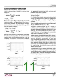
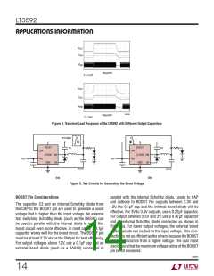
Figure 4. Transient Load Response of the LT3592 with Different Output Capacitors
D2
D2
OPTIONAL
C3
BOOST
BOOST
C3
CAP
CAP
LT3592 SW
LT3592 SW
V
V
IN
BATT
BATT
IN
GND
DA
GND
DA
3592 F05a
3592 F05b
(5a)
(5b)
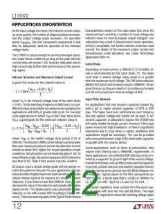
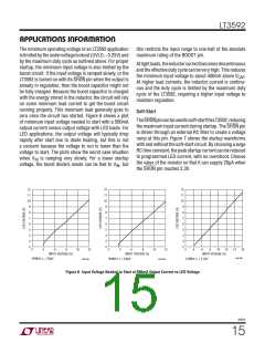
Figure 5. Two Circuits for Generating the Boost Voltage
BOOST Pin Considerations
parallel with the internal Schottky diode, anode to CAP
and cathode to BOOST. For outputs between 3.3V and
12V, the 0.1μF cap and the internal boost diode will be
effective. For 3V to 3.3V outputs, use a 0.22μF capacitor.
For output between 2.5V and 3V, use a 0.47μF capacitor
and an external Schottky diode connected as shown in
Figure 5a. For lower output voltages, the external boost
diode’s anode can be tied to the input voltage. This con-
nectionisnotasefficientastheothersbecausetheBOOST
pin current comes from a higher voltage. The user must
alsobesurethatthemaximumvoltageratingoftheBOOST
pin is not exceeded.
The capacitor C3 and an internal Schottky diode from
the CAP to the BOOST pin are used to generate a boost
voltage that is higher than the input voltage. An external
fast switching Schottky diode (such as the BAS40) can
be used in parallel with the internal diode to make this
boost circuit even more effective. In most cases, a 0.1μF
capacitor works well for the boost circuit. The BOOST pin
must be at least 2.5V above the SW pin for best efficiency.
For output voltages above 12V, use a 0.1μF cap and an
external boost diode (such as a BAS40) connected in
3592fc
14

 Linear Systems [ Linear Systems ]