LT3592
APPLICATIONS INFORMATION
ground the SHDN pin, the SW pin current will drop to es-
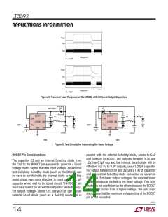
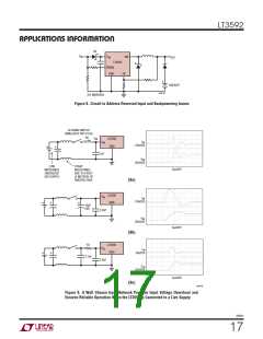
is minor, reducing it by less than one half percent for a two
red series LED load in BRIGHT mode operating from 32V.
sentially zero. However, if the V pin is grounded while
IN
the output is held high, then parasitic diodes inside the
Frequency Compensation
LT3592 can pull large currents from the output through
the SW pin and the V pin. Figure 8 shows a circuit that
IN
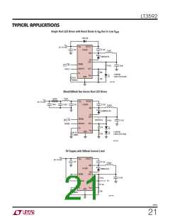
The LT3592 uses current mode control to regulate the
loop, whether the current control or voltage control loop
is active. This simplifies loop compensation. In particular,
the LT3592 does not require the ESR of the output capaci-
tor for stability, allowing the use of ceramic capacitors
to achieve low output ripple and small circuit size. A low
ESR output capacitor will typically provide for a greater
margin of circuit stability than an otherwise equivalent
capacitor with higher ESR, although the higher ESR will
tend to provide a faster loop response. Figure 10 shows
an equivalent circuit for the LT3592 control loops, both for
currentandvoltagemode.Bothusethesameerroramplifier
and power section, but an additional voltage gain amp is
used in conjuction with the external current sense resistor
to implement output current control. The error amplifier is
atransconductancetypewithfiniteoutputimpedance.The
power section, consisting of the modulator, power switch,
and inductor, is modeled as a transconductance amplifier
generating an output current proportional to the voltage
will run only when the input voltage is present and that
protects against a shorted or reversed input.
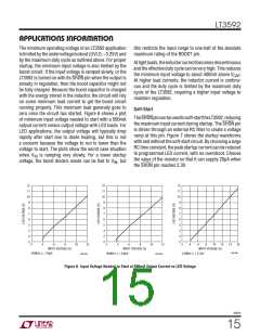
Hot Plugging Safely
Thesmallsize, robustness, andlowimpedanceofceramic
capacitors make them an attractive option for the input
bypasscapacitorofLT3592circuits.However,thesecapaci-
tors can cause problems if the LT3592 is plugged into a
live supply (see Linear Technology Application Note 88 for
a complete discussion). The low loss ceramic capacitor
combined with stray inductance in series with the power
source forms an underdamped tank circuit, and the volt-
age at the V pin of the LT35392 can ring to twice the
IN
nominal input voltage, possibly exceeding the LT3592’s
rating and damaging the part. If the input supply is poorly
controlled or the user will be plugging the LT3592 into an
energized supply, the input network should be designed
to prevent this overshoot.
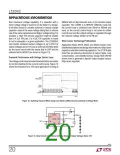
at the V node. Note that the output capacitor integrates
C
Figure 9 shows the waveforms that result when an LT3592
circuit is connected to a 32V supply through six feet of 24
gauge twisted pair. The first plot is the response with a 1μF
ceramic capacitor at the input. The input voltage rings as
high as 56V and the input current peaks at 16A.
this current, and that the capacitor on the V node (C )
C
C
integrates the error amplifier output current, resulting in
g
= 0.7A/V
m
–
0.7V
SW
One method of damping the tank circuit is to add another
capacitor with a series resistor to the circuit. In Figure 9b,
atantalumchipcapacitorhasbeenadded. Thiscapacitor’s
high equivalent series resistance (ESR) damps the circuit
and eliminates the voltage overshoot. The extra capacitor
improves low frequency ripple filtering and can slightly
improve the efficiency of the circuit, thought it is likely
to be the largest component in the circuit. An alternate
solution is shown in Figure 9c. A 1ꢀ resistor is added in
series with the input to eliminate the voltage overshoot
(it also reduces the peak input current). A 0.1μF capacitor
improves high frequency filtering. This solution is smaller
and less expensive than the tantalum capacitor. For high
input voltages, the impact of the 1ꢀ resistor on efficiency
+
+
C1
BRIGHT
CAP
C1
30k
ESR
–
300k
R
SENSE
OUT
+
R
L
–
–
+
R1
R2
g
= 1/5k
m
V
C
V
FB
1.2V
R
C
g
m
= 300μA/V
C
C
GND
3592 F10
Figure 10. Model for Loop Response
3592fc
18

 Linear Systems [ Linear Systems ]