LT3592
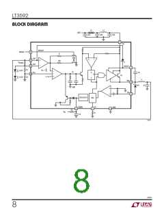
APPLICATIONS INFORMATION
(~0.4V at maximum load). This leads to a minimum input
voltage of:
the V absolute maximum range (36V) during overload
IN
conditions (short circuit or startup).
V
OUT + VD
Minimum On Time
V
=
– VD + VSW
IN(MIN)
DCMAX
The LT3592 will still regulate the output properly at input
voltages that exceed V
(up to 36V); however, the
IN(MAX)
with DC
= 0.90.
MAX
output voltage ripple increases as the input voltage is
The maximum input voltage is determined by the absolute
maximum ratings of the V and BOOST pins. The con-
tinuous mode operation, the maximum input voltage is
determinedbytheminimumdutycycle,whichisdependent
upon the oscillator frequency:
increased.
IN
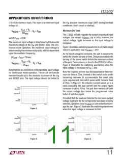
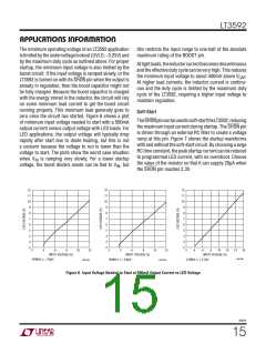
Figure1illustratesswitchingwaveformsina2.2MHzsingle
red LED application near V
= 24V.
IN(MAX)
As the input voltage is increased, the part is required to
switch for shorter periods of time. Delays associated with
turning off the power switch dictate the minimum on time
of the part. The minimum on time for the LT3592 is ~70ns.
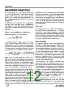
Figure 2 illustrates the switching waveforms when the
DC
= f
• 70nsec
OSC
MIN
V
OUT + VD
DCMIN
V
=
– VD + VSW
IN(MAX)
input voltage is increased to V = 26V.
IN
Notethatthisisarestrictionontheoperatinginputvoltage
for continuous mode operation. The circuit will tolerate
transient inputs up to the absolute maximum of the V
and BOOST pins. The input voltage should be limited to
Now the required on time has decreased below the mini-
mum on time of 70ns. Instead of the switch pulse width
becoming narrower to accommodate the lower duty
cycle requirement, the switch pulse width remains fixed
at 70ns. In Figure 2, the inductor current ramps up to a
value exceeding the load current and the output ripple
increases to about 70mV. The part then remains off until
the output voltage dips below the programmed value
before it switches again.
IN
V
OUT
50mV/DIV
I
L
500mA/DIV
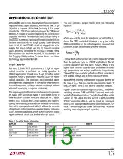
Provided that the load can tolerate the increases output
voltage ripple and the the components have been properly
V
SW
20V/DIV
selected,operationaboutV
issafeandwillnotdam-
3592 F01
IN(MAX)
1μs/DIV
age the part. Figure 3 illustrates the switching waveforms
when the input voltage is increased to 36V.
Figure 1.
V
V
OUT
OUT
50mV/DIV
50mV/DIV
I
L
I
L
500mA/DIV
500mA/DIV
V
V
SW
20V/DIV
SW
20V/DIV
3592 F02
3592 F03
1μs/DIV
1μs/DIV
Figure 2.
Figure 3.
3592fc
11

 Linear Systems [ Linear Systems ]