LT3592
PIN FUNCTIONS
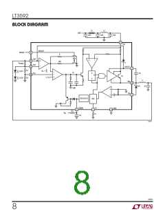
R (Pin1):Programsthefrequencyoftheinternaloscillator.
capacitor. An internal Schottky is provided for the boost
function and an external diode is not needed. An external
Schottky diode should be connected between BOOST and
CAP for single LED applications or whenever a higher
BOOST voltage is desired.
T
Connect a resistor from R to ground. Refer to Table 1 or
T
theTypicalPerformanceCharacteristicsforresistorvalues
that result in desired oscillator frequencies.
BRIGHT (Pin 2): Used to program a 10:1 dimming ratio
for theLED current. Drivethispinabove1.4Vtocommand
maximum intensity or below 0.3V to command minimum
intensity. This pin can be PWMed at 150Hz for brightness
control between the 1x and 10x current levels.
CAP (Pin 8): Output of the step-down converter and also
an input to the LED current sense amplifier. Connect the
filter capacitor, inductor, and the top of the external LED
current sense resistor to this pin.
SHDN (Pin 3): Used to shutdown the switching regulator
and the internal bias circuits. This pin can be PWMed at
150Hz for brightness control.
OUT (Pin 9): Drives the LED or LEDs and is the other
input to the LED current sense amplifier. Connect this pin
to the anode of the top LED in the string, the bottom of
the external LED current sense resistor, and the top of the
V (Pin 4): Supplies current to the LT3592’s internal cir-
IN
V
resistor divider.
FB
cuitry and to the internal power switches. Must be locally
bypassed.Forautomotiveapplications,apinetworkwitha
V
(Pin 10): The feedback node for the output voltage
FB
capfromV toGND, aseriesinductorconnectedbetween
controlloop.TiethisnodetoaresistordividerbetweenOUT
and GND to set the maximum output voltage of the step-
down converter according to the following formula:
IN
V and the power source, and another cap from the far
IN
end of the inductor to GND is recommended.
DA (Pin 5): Allows the external catch diode current to be
R1+R2
V
OUT =1.21•
sensed to prevent current runaway, such as when V is
IN
R2
high and the duty cycle is very low. Connect this pin to
the anode of the external catch Schottky diode.
whereR1connectsbetweenOUTandV andR2connects
between V and GND.
FB
FB
SW (Pin 6): The SW pin is the output of the internal power
switch. Connect this pin to the inductor and the cathode
of the switching diode.
Exposed Pad (Pin 11): Ground. The underside exposed
pad metal of the package provides both electrical contact
to ground and good thermal contact to the printed circuit
board. The device must be soldered to the circuit board
for proper operation.
BOOST (Pin 7): Provides a drive voltage, higher than the
input voltage to the internal bipolar NPN power switch.
BOOST will normally be tied to the SW pin through a 0.1μF
3592fc
7

 Linear Systems [ Linear Systems ]