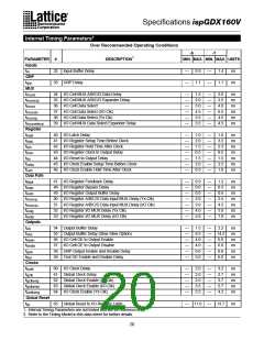
Specifications ispGDX160V
1
Internal Timing Parameters
Over Recommended Operating Conditions
-5
-7
1
PARAMETER
Inputs
#
DESCRIPTION
MIN. MAX. MIN. MAX. UNITS
t
32 Input Buffer Delay
33 GRP Delay
—
—
0.9
1.1
—
—
1.4
1.1
ns
ns
io
GRP
t
grp
MUX
t
t
t
t
t
t
34 I/O Cell MUX A/B/C/D Data Delay
35 I/O Cell MUX A/B/C/D Expander Delay
36 I/O Cell Data Select
—
—
—
—
—
—
1.5
2.0
3.0
4.5
3.5
3.5
—
—
—
—
—
—
2.0
2.5
4.0
6.5
4.5
4.5
ns
ns
ns
ns
ns
ns
muxd
muxexp
muxs
37 I/O Cell Data Select (I/O Clk)
38 I/O Cell Data Select (Yx Clk)
muxsio
muxsg
muxselexp
39 I/O Cell MUX Data Select Expander Delay
Register
t
t
t
t
t
t
t
40 I/O Latch Delay
—
—
—
—
—
—
—
1.0
2.0
1.5
0.5
1.5
2.0
0.5
—
—
—
—
—
—
—
1.0
3.2
2.3
0.5
1.5
2.5
1.0
ns
ns
ns
ns
ns
ns
ns
iolat
iosu
ioh
41 I/O Register Setup Time Before Clock
42 I/O Register Hold Time After Clock
43 I/O Register Clock to Output Delay
44 I/O Reset to Output Delay
ioco
ior
45 I/O Clock Enable Setup Time Before Clock
46 I/O Clock Enable Hold Time After Clock
cesu
ceh
Data Path
t
t
t
t
t
t
t
47 I/O Register Feedback Delay
—
—
—
—
—
—
—
0.9
0.0
0.0
2.0
3.0
4.0
5.0
—
—
—
—
—
—
—
1.2
0.3
0.6
2.5
4.5
5.0
7.0
ns
ns
ns
ns
ns
ns
ns
fdbk
48 I/O Register Bypass Delay
iobp
49 I/O Register Output Buffer Delay
ioob
50 I/O Register A/B/C/D Data Input MUX Delay (Yx Clk)
51 I/O Register A/B/C/D Data Input MUX Delay (I/O Clk)
52 I/O Register I/O MUX Delay (Yx Clk)
53 I/O Register I/O MUX Delay (I/O Clk)
muxcg
muxcio
iodg
iodio
Outputs
t
t
t
t
t
t
54 Output Buffer Delay
—
—
—
—
—
—
1.5
9.5
4.0
4.0
0.0
5.0
—
—
—
—
—
—
2.2
14.2
6.0
ns
ns
ns
ns
ns
ns
ob
55 Output Buffer Delay (Slow Slew Option)
56 I/O Cell OE to Output Enable
57 I/O Cell OE to Output Disable
58 GRP Output Enable and Disable Delay
59 Test OE Enable and Disable Delay
obs
oeen
oedis
goe
toe
6.0
0.0
6.0
Clocks
t
t
t
t
t
60 I/O Clock Delay
—
—
—
—
—
2.0
2.0
2.5
3.5
2.5
—
—
—
—
—
3.2
2.7
3.7
5.7
4.2
ns
ns
ns
ns
ns
ioclk
61 Global Clock Delay
gclk
62 Global Clock Enable (Yx Clk)
63 Global Clock Enable (I/O Clk)
64 I/O Clock Enable (Yx Clk)
gclkeng
gclkenio
ioclkeng
Global Reset
t
65 Global Reset to I/O Register Latch
—
11.0
—
13.7
ns
gr
1. Internal Timing Parameters are not tested and are for reference only.
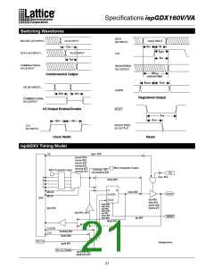
2. Refer to the Timing Model in this data sheet for further details.
20

 LATTICE [ LATTICE SEMICONDUCTOR ]