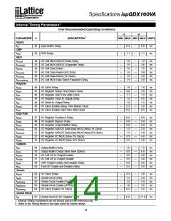
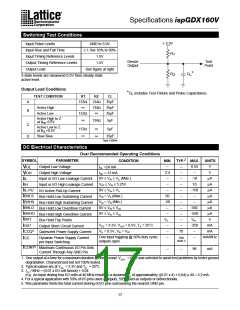
Specifications ispGDX160V
External Timing Parameters
Over Recommended Operating Conditions
-5
-7
TEST1
COND.
PARAMETER
#
DESCRIPTION
UNITS
MIN. MAX. MIN. MAX.
A
A
–
–
–
–
–
–
–
–
–
–
–
–
–
–
–
–
A
A
A
A
B
C
B
C
–
–
–
–
D
A
tpd
tsel
fmax (Tog.)
fmax (Ext.)
tsu1
tsu2
tsu3
tsu4
tsuce1
tsuce2
tsuce3
th1
th2
th3
Data Prop. Delay from Any I/O pin to Any I/O pin (4:1 MUX)
Data Prop. Delay from MUXsel Inputs to Any Output (4:1 MUX)
–
–
5.0
6.5
–
1
–
–
7.0
9.0
–
ns
ns
MHz
MHz
ns
ns
ns
ns
ns
ns
ns
ns
ns
ns
ns
ns
ns
ns
ns
ns
ns
ns
ns
ns
ns
ns
ns
ns
ns
ns
ns
ns
2
Clock Frequency, Max. Toggle
143
110
4.0
3.0
4.0
3.0
2.5
1.5
4.5
0.0
1.5
0.0
1.5
0.0
1.5
0.0
–
3
100
80.0
5.5
4.5
5.5
4.5
3.5
2.5
6.5
0.0
2.5
0.0
2.5
0.0
2.5
0.0
–
1
(
)
Clock Frequency with External Feedback
–
4
–
tsu3+tgco1
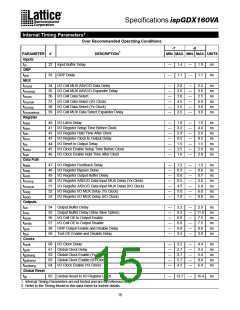
Input Latch or Register Setup Time Before Yx
Input Latch or Register Setup Time Before I/O Clock
Output Latch or Register Setup Time Before Yx
–
5
–
–
–
6
–
–
7
Output Latch or Register Setup Time Before I/O Clock
Global Clock Enable Setup Time Before Yx
Global Clock Enable Setup Time Before I/O Clock
I/O Clock Enable Setup Time Before Yx
Input Latch or Register Hold Time (Yx)
Input Latch or Register Hold Time (I/O Clock)
Output Latch or Register Hold Time (Yx)
Output Latch or Register Hold Time (I/O Clock)
Global Clock Enable Hold Time (Yx)
–
8
–
–
–
9
–
–
10
11
12
13
14
15
16
17
18
19
20
21
22
23
24
25
26
27
28
29
30
31
32
–
–
–
–
–
–
–
–
th4
–
–
thce1
thce2
thce3
tgco1
tgco2
tco1
tco2
ten
tdis
ttoeen
ttoedis
twh
twl
trst
trw
tsl
tsk
–
–
Global Clock Enable Hold Time (I/O Clock)
I/O Clock Enable Hold Time (Yx)
–
–
–
–
Output Latch or Register Clock (from Yx) to Output Delay
Input Latch or Register Clock (from Yx) to Output Delay
Output Latch or Register Clock (from I/O pin) to Output Delay
Input Latch or Register Clock (from I/O pin) to Output Delay
Input to Output Enable
5.0
8.5
6.0
9.5
6.0
6.0
9.0
9.0
–
7.0
11.0
9.0
13.0
8.5
8.5
12.0
12.0
–
–
–
–
–
–
–
–
–
Input to Output Disable
–
–
Test OE Output Enable
–
–
Test OE Output Disable
–
–
Clock Pulse Duration, High
3.5
3.5
–
5.0
5.0
–
Clock Pulse Duration, Low
–
–
Register Reset Delay from RESET Low
Reset Pulse Width
14.0
–
18.0
–
10.0
–
14.0
–
Output Delay Adder for Output Timings Using Slow Slew Rate
Output Skew (tgco1 Across Chip)
8.0
0.5
12.0
0.5
–
–
1. All timings measured with one output switching, fast output slew rate setting, except tsl.
18

 LATTICE [ LATTICE SEMICONDUCTOR ]