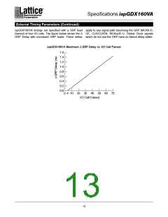
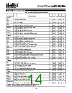
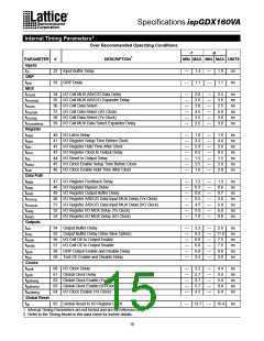
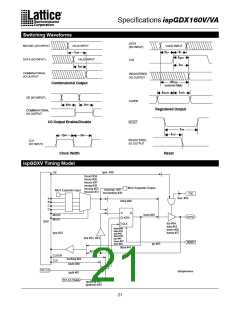
Specifications ispGDX160V
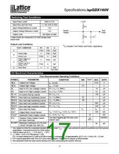
Switching Test Conditions
+ 3.3V
Input Pulse Levels
GND to 3.0V
≤ 1.5ns 10% to 90%
1.5V
Input Rise and Fall Time
Input Timing Reference Levels
Output Timing Reference Levels
Output Load
R
1
Device
Output
Test
Point
1.5V
See figure at right
R
2
C *
L
3-state levels are measured 0.5V from steady-state
active level.
Output Load Conditions
*C includes Test Fixture and Probe Capacitance.
L
TEST CONDITION
R1
153Ω
∞
R2
134Ω
134Ω
∞
CL
A
B
35pF
35pF
35pF
Active High
Active Low
153Ω
Active High to Z
∞
134Ω
5pF
5pF
at VOH-0.5V
C
D
Active Low to Z
at VOL+0.5V
153Ω
∞
∞
35pF
Table 2-0004A
Slow Slew
∞
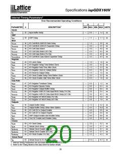
DC Electrical Characteristics
Over Recommended Operating Conditions
CONDITION
2
SYMBOL
PARAMETER
Output Low Voltage
Output High Voltage
MIN. TYP.
MAX.
0.55
–
UNITS
V
–
2.4
–
–
–
IOL =24 mA
VOL
VOH
IIL
V
IOH =-12 mA
0V ≤ VIN ≤ VIL (Max.)
-10
10
µA
–
Input or I/O Low Leakage Current
Input or I/O High Leakage Current
I/O Active Pull-Up Current
VCC ≤ VIN ≤ 5.25V
–
µA
–
IIH
0V ≤ VIN ≤ VIL
VIN = VIL (Max.)
VIN = VIH (Min.)
0V ≤ VIN ≤ VCC
0V ≤ VIN ≤ VCC
–
-150
–
µA
–
IIL-PU
IBHLS
IBHHS
IBHLO
IBHHO
IBHT
IOS1
50
-50
–
µA
–
Bus Hold Low Sustaining Current
Bus Hold High Sustaining Current
Bus Hold Low Overdrive Current
Bus Hold High Overdrive Current
Bus Hold Trip Points
–
–
µA
–
550
-550
VIH
-250
–
µA
–
µA
–
VIL
–
V
–
VCC = 3.3V, VOUT = 0.5V, TA = 25˚C
mA
mA
mA/MHz
–
Output Short Circuit Current
Quiescent Power Supply Current
ICCQ4
VIL = 0.5V, VIH = VCC
–
70
One input toggling @ 50% duty cycle,
outputs open.
–
–
Dynamic Power Supply Current
per Input Switching
See
ICC
Note 3
ICONT5
Maximum Continuous I/O Pin Sink
Current Through Any GND Pin
–
96
mA
–
1. One output at a time for a maximum duration of one second. VOUT = 0.5V was selected to avoid test problems by tester ground
degradation. Characterized but not 100% tested.
2. Typical values are at VCC = 3.3V and TA = 25oC.
3. ICC / MHz = (0.01 x I/O cell fanout) + 0.04
e.g. An input driving four I/O cells at 40 MHz results in a dynamic ICC of approximately ((0.01 x 4) + 0.04) x 40 = 3.2 mA.
4. For a typical application with 50% of I/O pins used as inputs, 50% used as outputs or bidirectionals.
5. This parameter limits the total current sinking of I/O pins surrounding the nearest GND pin.
17

 LATTICE [ LATTICE SEMICONDUCTOR ]