LANSDALE Semiconductor, Inc.
ML1451xx
ML14515X FAMILY CHARACTERISTICS AND DESCRIPTIONS - CONTINUED
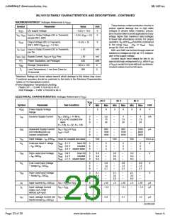
MAXIMUM RATINGS* (Voltages Referenced to V
)
SS
These devices contain protection circuitry to
Symbol
Parameter
DC Supply Voltage
Value
Unit
V
protect against damage due to high static
voltages or electric fields. However, precau-
tionsmust betakentoavoidapplicationsofany
voltage higher than maximum rated voltages
to these high–impedance circuits. For proper
V
DD
– 0.5 to + 10.0
V , V
in out
Input or Output Voltage (DC or Transient)
except SW1, SW2
– 0.5 to V
DD
+ 0.5
V
operation, V and V
to the range V
SS
except for SW1 and SW2.
SW1 and SW2 can be tied through external
resistors to voltages as high as 15 V, indepen-
dent of the supply voltage.
Unused inputs must always be tied to an
appropriatelogicvoltagelevel(e.g.,eitherV
should be constrained
V
Output Voltage (DC or Transient),
– 0.5 to + 15
10
V
in
out
out
(V or V
in out
)
V
DD
SW1, SW2 (R
= 4.7 kΩ)
pull–up
I , I
in out
Input or Output Current (DC or Transient),
per Pin
mA
I
, I
Supply Current, V
DD
or V
Pins
30
500
mA
mW
C
DD SS
SS
P
Power Dissipation, per Package†
Storage Temperature
D
SS
orV ),exceptforinputswithpull–updevices.
DD
Unused outputs must be left open.
T
stg
– 65 to + 150
260
T
Lead Temperature, 1 mm from Case for
10 seconds
C
L
* Maximum Ratings are those values beyond which damage to the device may occur.
Functional operation should be restricted to the limits in the Electrical Characteristics
tables or Pin Descriptions section.
†Power Dissipation Temperature Derating:
Plastic DIP: – 12 mW/ C from 65 to 85 C
SOG Package: – 7 mW/ C from 65 to 85 C
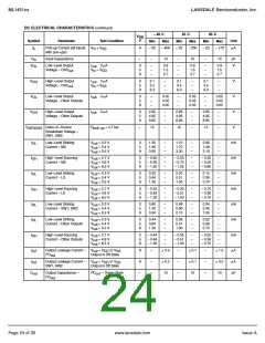
ELECTRICAL CHARACTERISTICS (Voltages Referenced to V
)
SS
– 40 C
25 C
Max
85 C
Max
V
DD
V
Symbol
Parameter
Test Condition
Unit
Min
Max
Min
Min
V
DD
Power Supply Voltage
Range
–
3
9
3
9
3
9
V
I
ss
Dynamic Supply Current
f
= OSC = 10 MHz,
3
5
9
–
–
–
3.5
10
30
–
–
–
3
7.5
24
–
–
–
3
7.5
24
mA
in
in
1 V p–p AC coupled sine
wave
R = 128, A = 32, N = 128
I
Quiescent Supply Current
(not including pull–up
current component)
V
= V
DD
= 0 µA
or V
SS
3
5
9
–
–
–
800
1200
1600
–
–
–
800
1200
1600
–
–
–
1600
2400
3200
µA
SS
in
I
out
V
Input Voltage – f , OSC
in
Input AC coupled sine wave
–
500
–
500
–
500
–
mV p–p
V
in
in
V
IL
LowLevel Input V oltage
– f , OSC
V
2.1 V
3.5 V
6.3 V square wave
Input DC
coupled
3
5
9
–
–
–
0
0
0
–
–
–
0
0
0
–
–
–
0
0
0
out
V
out
in
in
V
out
V
High–Level Input Voltage
– f , OSC
V
0.9 V
1.5 V
2.7 V square wave
Input DC
coupled
3
5
9
3.0
5.0
9.0
–
–
–
3.0
5.0
9.0
–
–
–
3.0
5.0
9.0
–
–
–
V
V
V
IH
out
V
out
in
in
V
out
V
Low–Level Input Voltage
– except f , OSC
3
5
9
–
–
–
0.9
1.5
2.7
–
–
–
0.9
1.5
2.7
–
–
–
0.9
1.5
2.7
IL
in
in
V
IH
High–Level Input Voltage
– except f , OSC
3
5
9
2.1
3.5
6.3
–
–
–
2.1
3.5
6.3
–
–
–
2.1
3.5
6.3
–
–
–
in
in
I
Input Current (f , OSC )
V
V
= V
= V
or V
SS
9
9
2
–
50
2
–
25
2
–
22
µA
µA
in
in
in
in
DD
SS
I
IL
Input Leakage Current
(Data, CLK, ENB –
without pull–ups)
– 0.3
– 0.1
– 1.0
in
I
IH
Input Leakage Current (all
V
in
= V
9
–
0.3
–
0.1
–
1.0
µA
DD
inputs except f , OSC )
in in
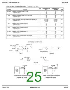
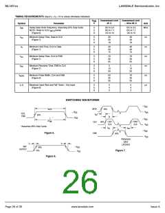
(continued)
Page 23 of 35
www.lansdale.com
Issue A

 LANSDALE [ LANSDALE SEMICONDUCTOR INC. ]