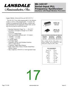
LANSDALE Semiconductor, Inc.
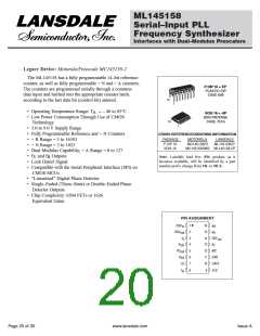
ML145158
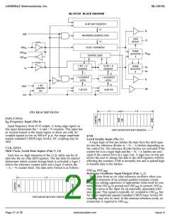
ML145158 BLOCK DIAGRAM
14–BIT SHIFT REGISTER
14
f
R
ENB
REFERENCE COUNTER LATCH
14
LOCK
DETECT
LD
PD
OSC
in
14–BIT
÷ RCOUNTER
PHASE
DETECTOR
A
OSC
out
out
out
CONTROL LOGIC
REF
7–BIT
COUNTER
÷
A
10–BIT ÷ N
PHASE
DETECTOR
B
φ
φ
V
f
in
COUNTER
R
7
10
÷
A COUNTER
LATCH
÷
N COUNTER
LATCH
f
V
7
10
1–BIT
CONTROL
S/R
DATA
CLK
MC
7–BIT S/R
10–BIT S/R
÷
A
÷
N
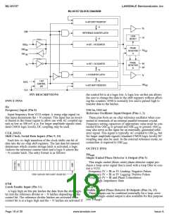
PIN DESCRIPTIONS
INPUT PINS
Frequency Input (Pin 8)
f
in
Input frequency from VCO output. A rising edge signal on
this input decrements the ÷ A and ÷ N counters. This input has
an inverter biased in the linear region to allow use with AC
coupled signals as low as 500 mV p–p. For larger amplitude
signals (standard CMOS logic levels), DC coupling may be
used.
FIRST DATA BIT INTO SHIFT REGISTER
ENB
Latch Enable Input (Pin 11)
A logic high on this pin latches the data from the shift regis-
ter into the reference divider or ÷ N, ÷ A latches depending on
the control bit. The reference divider latches are activated if the
control bit is at a logic high and the ÷ N, ÷ A latches are acti-
vated if the control bit is at a logic low. A logic low on this pin
allows the user to change the data in the shift registers without
affecting the counters. ENB is normally low and is pulsed high
to transfer data to the latches.
CLK, DATA
Shift Clock, Serial Data Inputs (Pins 9, 10)
Each low–to–high transition of the CLK shifts one bit of
data into the on–chip shift registers. The last data bit entered
determines which counter storage latch is activated; a logic 1
selects the reference counter latch and a logic 0 selects the
÷ A, ÷ N counter latch. The data entry format is as follows:
OSC , OSC
in
out
Reference Oscillator Input/Output (Pins 1, 2)
These pins form an on–chip reference oscillator when con-
nected to terminals of an external parallel resonant crystal.
Frequency setting capacitors of appropriate value must be con-
÷
R
nected from OSC to ground and OSC
to ground. OSC
in out
in
may also serve as the input for an externally–generated refer-
ence signal. This signal is typically AC coupled to OSC , but
in
for larger amplitude signals (standard CMOS logic levels) DC
coupling may also be used. In the external reference mode, no
FIRST DATA BIT INTO SHIFT REGISTER
connection is required to OSC
.
out
Page 21 of 35
www.lansdale.com
Issue A

 LANSDALE [ LANSDALE SEMICONDUCTOR INC. ]