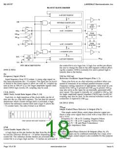
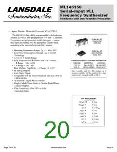
ML145158
LANSDALE Semiconductor, Inc.
ML145158
OUTPUT PINS
lus prescaler divide values respectively for high and low modu-
lus control levels, N the number programmed into the ÷ N
counter, and A the number programmed into the ÷ A counter.
Note that when a prescaler is needed, the dual–modulus ver-
sion offers a distinct advantage. The dual–modulus prescaler
allows a higher reference frequency at the phase detector input,
increasing system performance capability, and simplifying the
loop filter design.
PD
out
Phase Detector A Output (Pin 5)
This single–ended (three–state) phase detector output pro-
duces a loop–error signal that is used with a loop filter to con-
trol a VCO.
Frequency f > f or f Leading: Negative Pulses
V
R
V
V
Frequency f < f or f Lagging: Positive Pulses
V
R
f , f
R V
Frequency f = f and Phase Coincidence:
V
R
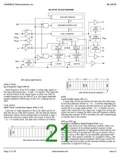
R Counter Output, N Counter Output (Pins 13, 3)
High–Impedance State
Buffered, divided reference and fin frequency outputs. The
φR, φV
f and f outputs are connected internally to the ÷ R and ÷ N
R
V
Phase Detector B Outputs (Pins 16, 15)
counter outputs respectively, allowing the counters to be used
independently, as well as monitoring the phase detector inputs.
Double–ended phase detector outputs. These outputs can be
combined externally for a loop–error signal. A single–ended
LD
output is also available for this purpose (see PD ).
out
Lock Detector Output (Pin 7)
If frequency f is greater than f or if the phase of f is
V
R
V
leading, then error information is provided by φ pulsing low.
This output is essentially at a high level when the loop is
V
φ remains essentially high.
locked (f , f of same phase and frequency), and pulses low
R
R V
If the frequency f is less than f or if the phase of f is
when loop is out of lock.
V
R
V
lagging, then error information is provided by φ pulsing low.
R
φ
remains essentially high.
REF
out
V
If the frequency of f = f and both are in phase, then both
Buffered Reference Oscillator Output (Pin 14)
V
R
φ
and φ remain high except for a small minimum time peri-
V
R
This output can be used as a second local oscillator, refer-
ence oscillator to another frequency synthesizer, or as the sys-
tem clock to a microprocessor controller.
od when both pulse low in phase.
MC
Dual–Modulus Prescaler Control Output (Pin 12)
POWER SUPPLY
This output generates a signal by the on–chip control logic
circuitry for controlling an external dual–modulus prescaler.
The MC level is low at the beginning of a count cycle and
remains low until the ÷ A counter has counted down from its
programmed value. At this time, MC goes high and remains
high until the ÷ N counter has counted the rest of the way
down from its programmed value (N – A additional counts
since both ÷ N and ÷ A are counting down during the first por-
tion of the cycle). MC is then set back low, the counters preset
to their respective programmed values, and the above sequence
repeated. This provides for a total programmable divide value
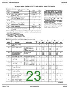
V
DD
Positive Power Supply (Pin 4)
The positive power supply potential. This pin may range
from + 3 to + 9 V with respect to VSS.
V
SS
Negative Power Supply (Pin 6)
The most negative supply potential. This pin is usually-
ground.
(N ) = N • P + A where P and P + 1 represent the dual–modu-
T
Page 22 of 35
www.lansdale.com
#

 LANSDALE [ LANSDALE SEMICONDUCTOR INC. ]