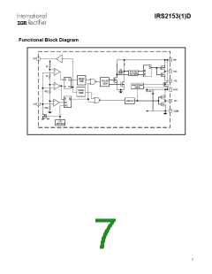
IRS2153(1)D
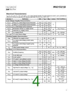
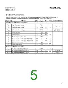
Electrical Characteristics
V
(V , V ) = 14 V, C = 1 nF, V =0 V and T = 25 °C unless otherwise specified. The output voltage and current (VO and IO)
BIAS CC BS
T
S
A
parameters are referenced to COM and are applicable to the respective output leads: HO or LO. CLO = CHO = 1 nF.
Test Conditions
Symbol
Definition
Min
Typ
Max Units
Gate Driver Output Characteristics
VOH
VOL
VCC
High-level output voltage
Low-level output voltage
---
---
---
IO = 0 A
COM
---
V
IO = 0 A
VCC ≤ VCCUV-
,
VOL_UV
UV-mode output voltage
---
COM
---
Output rise time
---
---
120
50
220
tr
tf
ns
Output fall time
80
---
Shutdown propagation delay
Output deadtime (HO or LO) (IRS2153D)
---
350
1.1
tsd
td
0.65
1.75
µs
µs
Output deadtime (HO or LO) (IRS21531D)
Output source current
0.35
---
0.6
180
260
0.85
---
td
IO+
IO-
mA
Output sink current
---
---
Bootstrap FET Characteristics
VB_ON
IB_CAP
IB_10V
VB when the bootstrap FET is on
VB source current when FET is on
VB source current when FET is on
---
40
10
13.7
55
---
---
---
V
CBS=0.1 uF
VB=10 V
mA
12
5

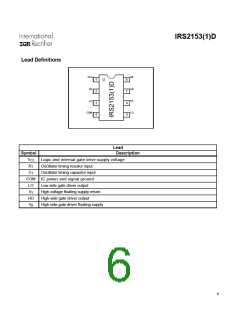
 INFINEON [ Infineon ]