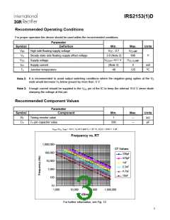
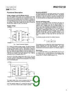
IRS2153(1)D
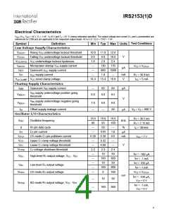
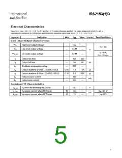
Electrical Characteristics
VBIAS (VCC, VBS) = 14 V, CT = 1 nF, VS=0 V and TA = 25 °C unless otherwise specified. The output voltage and current (VO and IO) parameters are
referenced to COM and are applicable to the respective output leads: HO or LO. CLO = CHO = 1 nF.
Test Conditions
Symbol
Definition
Min Typ Max Units
Low Voltage Supply Characteristics
VCCUV
+
Rising VCC undervoltage lockout threshold
Falling VCC undervoltage lockout threshold
10.0
8.0
1.6
---
11.0
9.0
12.0
10.0
2.4
V
VCCUV
-
VCCUVHYS VCC undervoltage lockout hysteresis
2.0
IQCCUV
IQCC
ICC
Micropower startup VCC supply current
Quiescent supply current
130
800
1.8
170
1000
---
VCC ≤ VCCUV-
µA
---
VCC
supply current
---
mA
V
RT = 36.9 kΩ
VCC
VCC zener clamp voltage
Floating Supply Characteristics
VCC
14.4
15.4
16.8
ICC = 5 mA
CLAMP
IQBS
Quiescent VBS supply current
BS supply undervoltage positive going
threshold
BS supply undervoltage negative going
---
60
80
µA
V
V
VBSUV+
8.0
9.0
9.5
V
VBSUV-
ILK
7.0
---
8.0
---
9.0
50
threshold
Offset supply leakage current
VB = VS = 600 V
µA
Oscillator I/O Characteristics
18.4
88
---
19.0
93
19.6
100
---
RT = 36.5 kΩ
RT = 7.15 kΩ
fo < 100 kHz
fOSC
Oscillator frequency
kHz
%
d
RT pin duty cycle
50
0.02
0.30
9.32
4.66
2.3
10
ICT
CT pin current
---
1.0
0.6
---
µA
ICTUV
VCT+
VCT-
VCTSD
UV-mode CT pin pulldown current
Upper CT ramp voltage threshold
Lower CT ramp voltage threshold
CT voltage shutdown threshold
0.20
---
mA
VCC = 7 V
V
---
---
2.2
---
2.4
50
IRT = -100 µA
IRT = -1 mA
IRT = 100 µA
IRT = 1 mA
VRT+
High-level RT output voltage, VCC - VRT
---
100
10
300
50
---
VRT-
Low-level RT output voltage
UV-mode RT output voltage
---
100
0
300
100
VRTUV
---
VCC ≤ VCCUV-
mV
IRT = -100 µA,
---
---
10
50
VCT = 0 V
VRTSD
SD-mode RT output voltage, VCC - VRT
IRT = -1 mA,
VCT = 0 V
100
300
4

 INFINEON [ Infineon ]