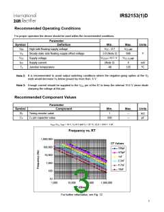
IRS2153(1)D
Recommended Operating Conditions
For proper operation the device should be used within the recommended conditions.
Parameter
Symbol
VBS
Definition
High side floating supply voltage
Steady state side floating supply offset voltage
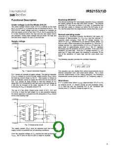
Supply voltage
Min.
VCC - 0.7
-3.0 (Note 2)
VCCUV+ +0.1 V
(Note 3)
Max.
VCLAMP
600
Units
V
VS
VCC
ICC
VCC CLAMP
5
Supply current
mA
ºC
TJ
Junction temperature
-40
125
It is recommended to avoid output switching conditions where the negative-going spikes at the VS
node would decrease VS below ground by more than -5 V.
Note 2:
Note 3:
Enough current should be supplied to the
clamping the voltage at this pin.
pin of the IC to keep the internal 15.6 V zener diode
VCC
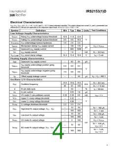
Recommended Component Values
Parameter
Symbol
RT
Component
Min.
1
Max.
---
Units
kΩ
Timing resistor value
CT pin capacitor value
CT
330
---
pF
VBIAS (VCC, VBS) = 14 V, VS=0 V and TA = 25 °C, CLO = CHO = 1 nF.
Frequency vs. RT
1,000,000
CT Values
100,000
10,000
1,000
100
330pf
470pF
1nF
2.2nF
4.7nF
10nF
10
1,000
10,000
100,000
1,000,000
RT (Ohm)
For further information, see Fig. 12.
3

 INFINEON [ Infineon ]