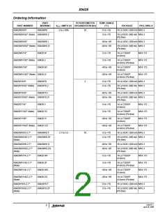
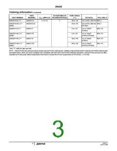
X9428
PRINCIPLES OF OPERATION
The X9428 is highly integrated microcircuit
incorporating a resistor array and its associated
registers and counters and the serial interface logic
providing direct communication between the host and
the XDCP potentiometers.
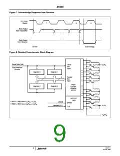
The X9428 will respond with an acknowledge after
recognition of a start condition and its slave address
and once again after successful receipt of the
command byte. If the command is followed by a data
byte the X9428 will respond with a final acknowledge.
a
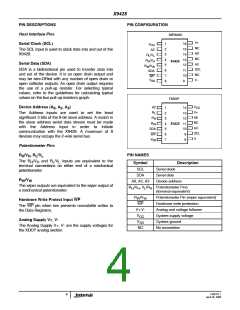
Array Description
The X9428 is comprised of a resistor array. The array
contains 63 discrete resistive segments that are
connected in series. The physical ends of the array
are equivalent to the fixed terminals of a mechanical
Serial Interface
The X9428 supports a bidirectional bus oriented
protocol. The protocol defines any device that sends
data onto the bus as a transmitter and the receiving
device as the receiver. The device controlling the
transfer is a master and the device being controlled is
the slave. The master will always initiate data transfers
and provide the clock for both transmit and receive
operations. Therefore, the X9428 will be considered a
slave device in all applications.
potentiometer (V /R and V /R inputs).
H
H
L
L
At both ends of the array and between each resistor
segment is a CMOS switch connected to the wiper
(V /R ) output. Within each individual array only one
W
W
switch may be turned on at a time. These switches are
controlled by the Wiper Counter Register (WCR). The
six bits of the WCR are decoded to select, and enable,
one of sixty-four switches.
Clock and Data Conventions
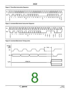
Data states on the SDA line can change only during
SCL LOW periods (tLOW). SDA state changes during
SCL HIGH are reserved for indicating start and stop
conditions.
The WCR may be written directly, or it can be changed
by transferring the contents of one of four associated
Data Registers into the WCR. These Data Registers and
the WCR can be read and written by the host system.
Start Condition
Device Addressing
All commands to the X9428 are preceded by the start
condition, which is a HIGH to LOW transition of SDA
while SCL is HIGH (t
monitors the SDA and SCL lines for the start condition
and will not respond to any command until this
condition is met.
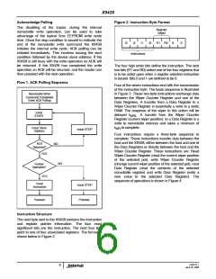
Following a start condition the master must output the
address of the slave it is accessing. The most
significant four bits of the slave address are the device
type identifier (refer to Figure 1 below). For the X9428
this is fixed as 0101[B].
). The X9428 continuously
HIGH
Figure 1. Slave Address
Stop Condition
Device Type
Identifier
All communications must be terminated by a stop
condition, which is a LOW to HIGH transition of SDA
while SCL is HIGH.
0
1
0
1
A3
A2
0
A0
Acknowledge
Acknowledge is a software convention used to provide
a positive handshake between the master and slave
devices on the bus to indicate the successful receipt of
data. The transmitting device, either the master or the
slave, will release the SDA bus after transmitting eight
bits. The master generates a ninth clock cycle and
during this period the receiver pulls the SDA line LOW
to acknowledge that it successfully received the eight
bits of data.
Device Address
The next four bits of the slave address are the device
address. The physical device address is defined by
the state of the A , A , A inputs. The X9428
0
2
3
compares the serial data stream with the address
input state; a successful compare of all four address
bits is required for the X9428 to respond with an
acknowledge. The A , A , A inputs can be actively
0
2
3
driven by CMOS input signals or tied to V
or V
.
CC
SS
FN8197.1
April 26, 2006
5

 INTERSIL [ Intersil ]