X9428
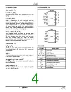
PIN DESCRIPTIONS
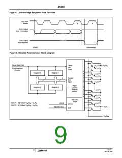
Host Interface Pins
Serial Clock (SCL)
PIN CONFIGURATION
DIP/SOIC
X9428
V+
NC
A0
1
2
3
4
5
6
7
8
16
15
14
13
12
11
10
9
V
CC
A2
The SCL input is used to clock data into and out of the
X9428.
R /V
L
L
NC
A3
R /V
H
H
Serial Data (SDA)
R
/V
W
W
SCL
NC
V-
SDA is a bidirectional pin used to transfer data into
and out of the device. It is an open drain output and
may be wire-ORed with any number of open drain or
open collector outputs. An open drain output requires
the use of a pull-up resistor. For selecting typical
values, refer to the guidelines for calculating typical
values on the bus pull-up resistors graph.
SDA
WP
V
SS
TSSOP
X9428
V
Device Address (A , A , A )
A2
CC
1
2
3
4
5
6
7
14
13
12
11
10
9
0
2
3
R
L
V+
The Address inputs are used to set the least
significant 3 bits of the 8-bit slave address. A match in
the slave address serial data stream must be made
with the Address input in order to initiate
communication with the X9428. A maximum of 8
devices may occupy the 2-wire serial bus.
A0
R
H
NC
A3
R
W
SDA
WP
SCL
V-
V
8
SS
Potentiometer Pins
PIN NAMES
R /V , R /V
L
H
H
L
The R /V and R /V inputs are equivalent to the
terminal connections on either end of a mechanical
potentiometer.
H
H
L
L
Symbol
SCL
Description
Serial clock
Serial data
SDA
R /V
W
W
A0, A2, A3
Device address
The wiper outputs are equivalent to the wiper output of
a mechanical potentiometer.
R /V , V /R
Potentiometer Pins
(terminal equivalent)
H
H
L
H
R /V
W
Potentiometer Pin (wiper equivalent)
Hardware write protection
Analog and voltage follower
System supply voltage
System ground
W
Hardware Write Protect Input WP
WP
The WP pin when low prevents nonvolatile writes to
the Data Registers.
V+,V-
V
CC
Analog Supply V+, V-
V
SS
NC
The Analog Supply V+, V- are the supply voltages for
the XDCP analog section.
No connection
FN8197.1
April 26, 2006
4

 INTERSIL [ Intersil ]