ISL88731A
information is added to the feedback to create a second zero
Compensation Break Frequency Equations
F
. The low pass filter R , C between R and
ZERO2 F2 F2 S2
1
----------------------------------------------------------------------
ISL88731A add a pole at F
. R and R are internal
F
=
FILTER
divider resistors that set the DC output voltage. For a 3-cell
battery, R = 500kΩ and R = 100kΩ. Equations 23 through
3
4
ZERO1
(2π ⋅ C
⋅ R
)
1COMP
VCOMP
(EQ. 23)
3
4
R
R
4
⎛
⎜
⎝
⎞
⎟
⎠
⎛
⎜
⎝
⎞
⎟
⎠
gm1
5
VCOMP
⎛
⎝
⎞
⎠
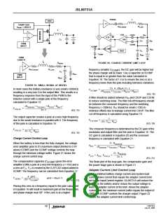
30 relate the compensation network’s poles, zeros and gain
to the components in Figure 23. Figure 25 shows an
asymptotic Bode plot of the DC/DC converter’s gain vs
frequency. It is strongly recommended that FZERO1 is
approximately 30% of FLC and FZERO2 is approximately 70%
----------------------------------------------
--------------------
-----------
F
F
=
⋅
⋅
ZERO2
2π ⋅ R
⋅ C
R
+ R
3
(EQ. 24)
(EQ. 25)
SENSE
4
o
1
-------------------------------
=
LC
(2π L ⋅ C )
o
1
------------------------------------------
=
F
F
FILTER
POLE1
(2π ⋅ R ⋅ C
)
F2
of FLC
.
(EQ. 26)
(EQ. 27)
F2
1
---------------------------------------------------
=
(2π ⋅ R
⋅ C )
o
SENSE
1
NO BATTERY
-------------------------------------------
F
=
ESR
(2π ⋅ C ⋅ R
)
ESR
(EQ. 28)
o
R
BATTERY
= 200mΩ
Choose R
VCOMP
from Equation 29.
equal or lower than the value calculated
R
BATTERY
= 50mΩ
R
+ R
4
R
4
⎛
⎜
⎝
⎞
⎟
⎠
5
gm1
3
⎛
⎝
⎞
⎠
-----------
--------------------
R
= (0.7 ⋅ F ) ⋅ (2π ⋅ C ⋅ R ) ⋅
SENSE
⋅
VCOMP
LC
o
(EQ. 29)
Next choose C
equal or higher than the value
VCOMP
calculated from Equation 30.
1
--------------------------------------------------------------------------
=
C
VCOMP
(0.3 ⋅ F ) ⋅ (2π ⋅ R
LC
)
VCOMP
(EQ. 30)
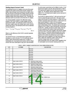
PCB Layout Considerations
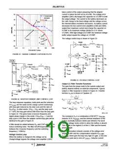
FREQUENCY
Power and Signal Layers Placement on the PCB
FIGURE 24. FREQUENCY RESPONSE OF THE LC OUTPUT
FILTER
As a general rule, power layers should be close together,
either on the top or bottom of the board, with signal layers on
the opposite side of the board. As an example, layer
arrangement on a 4-layer board is shown below:
1. Top Layer: signal lines, or half board for signal lines and
the other half board for power lines
60
Compensator
Modulator
2. Signal Ground
40
20
Loop
FPOLE1
FFILTER
ESR
3. Power Layers: Power Ground
F
LC
4. Bottom Layer: Power MOSFET, Inductors and other
Power traces
Separate the power voltage and current flowing path from
the control and logic level signal path. The controller IC will
stay on the signal layer, which is isolated by the signal
ground to the power signal traces.
0
-20
-40
-60
F
Component Placement
ZERO1
F
ZERO2
The power MOSFET should be close to the IC so that the
gate drive signal, the LGATE, UGATE, PHASE, and BOOT,
traces can be short.
F
0.1
1
10
FREQUENCY (kHz)
100
1000
Place the components in such a way that the area under the
IC has less noise traces with high dv/dt and di/dt, such as
gate signals and phase node signals.
FIGURE 25. ASYMPTOTIC BODE PLOT OF THE VOLTAGE
CONTROL LOOP GAIN
FN6738.0
July 23, 2008
20

 INTERSIL [ Intersil ]