ISL88731A
the lower byte stored in that register. After receiving the byte,
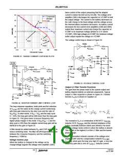
Charger Timeout
the master Acknowledges by holding SDA low during the 9th
clock pulse. ISL88731A then sends the higher byte stored in
the register. After the second byte, neither device holds SDA
low (No Acknowledge). The master will then produce a Stop
condition to end the read transaction.
The ISL88731A includes 2 timers to insure the SMBus
master is active and to prevent overcharging the battery.
ISL88731A will terminate charging if the charger has not
received a write to the ChargeVoltage or ChargeCurrent
register within 175s or if the SCL line is low for more than
25ms. If a time-out occurs, either ChargeVoltage or
ChargeCurrent registers must be written to re-enable
charging.
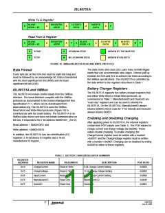
ISL88731A does not support reading more than 1 register
per transaction.
Application Information
ISL88731A Data Byte Order
The following battery charger design refers to the ”Typical
Application Circuit” (see Figure 2), where typical battery
configuration of 3S2P is used. This section describes how to
select the external components including the inductor, input
and output capacitors, switching MOSFETs and current
sensing resistors.
Each register in ISL88731A contains 16bits or 2, 8 bit bytes.
All data sent on the SMBus is in 8-bit bytes and 2 bytes must
be written or read from each register in ISL88731A. The
order in which these bytes are transmitted appears reversed
from the way they are normally written. The LOW byte is
sent first and the HI byte is sent second. For example, When
writing 0x41A0, 0xA0 is written first and 0x41 is sent second.
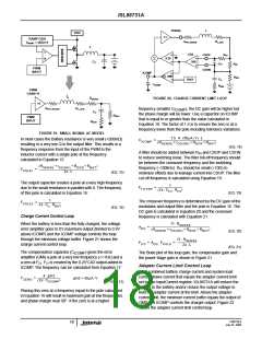
Inductor Selection
The inductor selection has trade-offs between cost, size,
crossover frequency and efficiency. For example, the lower
the inductance, the smaller the size, but ripple current is
higher. This also results in higher AC losses in the magnetic
core and the windings, which decreases the system
Writing to the Internal Registers
In order to set the charge current, charge voltage or input
current, valid 16-bit numbers must be written to ISL88731A’s
internal registers via the SMBus.
efficiency. On the other hand, the higher inductance results
in lower ripple current and smaller output filter capacitors,
but it has higher DCR (DC resistance of the inductor) loss,
lower saturation current and has slower transient response.
So, the practical inductor design is based on the inductor
ripple current being ±15% to ±20% of the maximum
To write to a register in the ISL88731A, the master sends a
control byte with the R/W bit set to 0, indicating a write. If it
receives an Acknowledge from the ISL88731A it sends a
register address byte setting the register to be written (i.e.
0x14 for the ChargeCurrent register). The ISL88731A will
respond with an Acknowledge. The master then sends the
lower data byte to be written into the desired register. The
ISL88731A will respond with an Acknowledge. The master
then sends the higher data byte to be written into the desired
register. The ISL88731A will respond with an Acknowledge.
The master then issues a Stop condition, indicating to the
ISL88731A that the current transaction is complete. Once
this transaction completes, the ISL88731A will begin
operating at the new current or voltage.
operating DC current at maximum input voltage. Maximum
ripple is at 50% duty cycle or V
= V /2. The
BAT
IN,MAX
required inductance for ±15% ripple current can be
calculated from Equation 3:
V
IN, MAX
--------------------------------------------------------
L =
4 ⋅ F
⋅ 0.3 ⋅ I
(EQ. 3)
is the
SW
SW
L, MAX
Where, V
is the maximum input voltage, F
IN,(MAX)
switching frequency and I
the inductor.
is the max DC current in
L,(MAX)
ISL88731A does not support writing more than one register
per transaction.
For V
= 20V, V
BAT
= 12.6V, I
= 4.5A, and
BAT,(MAX)
IN,(MAX)
f = 400kHz, the calculated inductance is 9.3µH. Choosing
s
Reading from the Internal Registers
The ISL88731A has the ability to read from 5 internal
the closest standard value gives L = 10µH. Ferrite cores are
often the best choice since they are optimized at 400kHz to
600kHz operation with low core loss. The core must be large
registers. Prior to reading from an internal register, the master
must first select the desired register by writing to it and
sending the registers address byte. This process begins by
the master sending a control byte with the R/W bit set to 0,
indicating a write. Once it receives an Acknowledge from the
ISL88731A it sends a register address byte representing the
internal register it wants to read. The ISL88731A will respond
with an Acknowledge. The master must then respond with a
Stop condition. After the Stop condition, the master follows
with a new Start condition, then sends a new control byte with
the ISL88731A slave address and the R/W bit set to 1,
indicating a read. The ISL88731A will Acknowledge then send
enough not to saturate at the peak inductor current I
Equation 4:
in
Peak
1
2
--
I
= I
+
⋅ I
RIPPLE
PEAK
L, MAX
(EQ. 4)
Inductor saturation can lead to cascade failures due to very
high currents. Conservative design limits the peak and RMS
current in the inductor to less than 90% of the rated
saturation current.
Crossover frequency is heavily dependent on the inductor
value. F
should be less than 20% of the switching
CO
FN6738.0
July 23, 2008
15

 INTERSIL [ Intersil ]