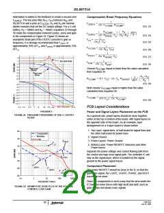
ISL88731A
frequency and a conservative design has F
less than
charger application, the input voltage of the synchronous
CO
10% of the switching frequency. The highest F
is in
buck converter is equal to the AC-adapter output voltage,
which is relatively constant. The maximum efficiency is
achieved by selecting a high-side MOSFET that has the
conduction losses equal to the switching losses. Switching
losses in the low-side FET are very small. The choice of
low-side FET is a trade-off between conduction losses
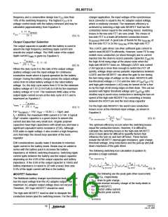
CO
voltage control mode with the battery removed and may be
calculated (approximately) from Equation 5:
5 ⋅ 11 ⋅ R
SENSE
------------------------------------------
=
F
CO
2π ⋅ L
(EQ. 5)
(r
) and cost. A good rule of thumb for the r
of
DS(ON)
the low-side FET is 2x the r
DS(ON)
Output Capacitor Selection
of the high-side FET.
DS(ON)
The output capacitor in parallel with the battery is used to
absorb the high frequency switching ripple current and
smooth the output voltage. The RMS value of the output
The LGATE gate driver can drive sufficient gate current to
switch most MOSFETs efficiently. However, some FETs may
exhibit cross conduction (or shoot-through) due to current
ripple current I
is given by Equation 6:
RMS
injected into the drain-to-source parasitic capacitor (C ) by
gd
V
IN, MAX
the high dV/dt rising edge at the phase node when the
high-side MOSFET turns on. Although LGATE sink current
(1.8A typical) is more than enough to switch the FET off
quickly, voltage drops across parasitic impedances between
LGATE and the MOSFET can allow the gate to rise during
the fast rising edge of voltage on the drain. MOSFETs with
low threshold voltage (<1.5V) and low ratio of C /C (<5)
and high gate resistance (>4Ω) may be turned on for a few
ns by the high dV/dt (rising edge) on their drain. This can be
avoided with higher threshold voltage and C /C ratio.
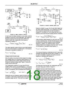
-----------------------------------
⋅ D ⋅ (1 – D)
I
=
RMS
12 ⋅ L ⋅ F
(EQ. 6)
SW
Where the duty cycle D is the ratio of the output voltage
(battery voltage) over the input voltage for continuous
conduction mode which is typical operation for the battery
charger. During the battery charge period, the output voltage
varies from its initial battery voltage to the rated battery
voltage. So, the duty cycle varies from 0.53 for the minimum
battery voltage of 7.5V (2.5V/Cell) to 0.88 for the maximum
battery voltage of 12.6V. The maximum RMS value of the
output ripple current occurs at the duty cycle of 0.5 and is
expressed as Equation 7:
gs gd
gs gd
Another way to avoid cross conduction is slowing the turn-on
speed of the high-side MOSFET by connecting a resistor
between the BOOT pin and the boot strap capacitor.
V
IN, MAX
-------------------------------------------
I
=
RMS
For the high-side MOSFET, the worst-case conduction
losses occur at the minimum input voltage, as shown in
Equation 8:
4 ⋅ 12 ⋅ L ⋅ F
(EQ. 7)
SW
For V
= 19V, V = 16.8V, L = 10µH, and
BAT
IN,(MAX)
f = 400kHz, the maximum RMS current is 0.19A. A typical
s
V
2
OUT
---------------
(EQ. 8)
20µF ceramic capacitor is a good choice to absorb this
current and also has very small size. Organic polymer
capacitors have high capacitance with small size and have a
significant equivalent series resistance (ESR). Although
ESR adds to ripple voltage, it also creates a high frequency
zero that helps the closed loop operation of the buck
regulator.
P
=
⋅ I
⋅ r
BAT DS(ON)
Q1, conduction
V
IN
The optimum efficiency occurs when the switching losses
equal the conduction losses. However, it is difficult to
calculate the switching losses in the high-side MOSFET
since it must allow for difficult-to-quantify factors that
influence the turn-on and turn-off times. These factors
include the MOSFET internal gate resistance, gate charge,
threshold voltage, stray inductance and the pull-up and pull-
down resistance of the gate driver.
EMI considerations usually make it desirable to minimize
ripple current in the battery leads. Beads may be added in
series with the battery pack to increase the battery
impedance at 400kHz switching frequency. Switching ripple
current splits between the battery and the output capacitor
depending on the ESR of the output capacitor and battery
impedance. If the ESR of the output capacitor is 10mΩ and
battery impedance is raised to 2Ω with a bead, then only
0.5% of the ripple current will flow in the battery.
The following switching loss calculation (Equation 9)
provides a rough estimate.
P
=
Q1, Switching
Q
Q
gd
⎛
⎞
⎟
⎠
⎛
⎜
⎝
⎞
⎟
⎠
1
1
2
gd
--
------------------------
--
-----------------
V
I
f
+
V
I
f
+ Q V f
rr IN sw
⎜
⎝
IN LV sw
IN LP sw
2
I
I
g, source
g, sink
(EQ. 9)
Where, the following are the peak gate-drive source/sink
current of Q , respectively:
MOSFET Selection
1
The Notebook battery charger synchronous buck converter
has the input voltage from the AC-adapter output. The
maximum AC-adapter output voltage does not exceed 25V.
Therefore, 30V logic MOSFET should be used.
• Q : drain-to-gate charge,
gd
• Q : total reverse recovery charge of the body-diode in
rr
low-side MOSFET,
• I : inductor valley current,
LV
• I : Inductor peak current,
LP
The high-side MOSFET must be able to dissipate the
conduction losses plus the switching losses. For the battery
• I
g,sink
• I ,
g source
FN6738.0
July 23, 2008
16

 INTERSIL [ Intersil ]