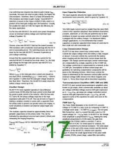
ISL88731A
L
L
PHASE
PHASE
VDD
11
11
RAMP GEN
RRFET_RDSON
FET_RDSON
RRL_DCR
L_DCR
VRAMP = VDD/11
L
-
+
CA2
CA2
R
CSOP
CSOP
R
+
+
F2
F2
Σ
0.25
0.25
+
S
+
S
Σ
20X
20X
CO
-
-
C
C
R
R
S2
S2
F2
F2
-
-
PWM
INPUT
CSON
CSON
ICOMP
ICOMP
-
-
GMI
GMI
R
RBAT
BAT
C
COO
DACI
DACI
+
+
CICOMP
CICOMP
RESR
RESR
PWM
GAIN=11
L
RSENSE
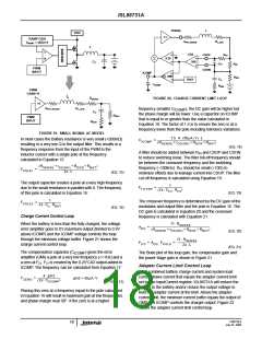
FIGURE 20. CHARGE CURRENT LIMIT LOOP
11
RFET_RDSON
RL_DCR
frequency (smaller C
), the DC gain will be higher but
ICOMP
CO
the phase margin will be lower. Use a capacitor on ICOMP
that is equal to or greater than the value calculated in
Equation 18. The factor of 1.5 is to ensure the zero is at a
frequency lower than the pole including tolerance variations.
RBAT
PWM
INPUT
RESR
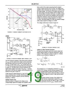
FIGURE 19. SMALL SIGNAL AC MODEL
1.5 ⋅ 4 ⋅ (50μA ⁄ V) ⋅ L
In most cases the Battery resistance is very small (<200mΩ)
resulting in a very low Q in the output filter. This results in a
frequency response from the input of the PWM to the
inductor current with a single pole at the frequency
calculated in Equation 15:
------------------------------------------------------------------------------------------------------
=
C
ICOMP
(R
+ r
+ R
+ R
)
BAT
SENSE
DS(ON)
DCR
(EQ. 18)
A filter should be added between RS2 and CSOP and CSON
to reduce switching noise. The filter roll-off frequency should
be between the crossover frequency and the switching
frequency (~100kHz). RF2 should be small (<10Ω) to
minimize offsets due to leakage current into CSOP. The filter
cut off frequency is calculated using Equation 19:
(R
+ r
+ R
+ R
)
BAT
SENSE
DS(ON)
DCR
------------------------------------------------------------------------------------------------------
=
F
POLE1
2π ⋅ L
(EQ. 15)
The output capacitor creates a pole at a very high frequency
due to the small resistance in parallel with it. The frequency
of this pole is calculated in Equation 16:
1
------------------------------------------
F
=
FILTER
(2π ⋅ C ⋅ R
)
F2
F2
(EQ. 19)
1
The crossover frequency is determined by the DC gain of the
modulator and output filter and the pole in Equation 16. The
DC gain is calculated in Equation 20 and the crossover
frequency is calculated with Equation 21:
--------------------------------------
F
=
POLE2
2π ⋅ C ⋅ R
o
BAT
(EQ. 16)
Charge Current Control Loop
When the battery is less than the fully charged, the voltage
error amplifier goes to it’s maximum output (limited to 0.3V
above ICOMP) and the ICOMP voltage controls the loop
through the minimum voltage buffer. Figure 21 shows the
charge current control loop.
11 ⋅ R
SENSE
------------------------------------------------------------------------------------------------------
=
A
DC
(R
+ r
+ R
+ R
)
BAT
SENSE
DS(ON)
DCR
(EQ. 20)
11 ⋅ R
SENSE
2π ⋅ L
----------------------------------
=
POLE
F
= A
⋅ F
CO
DC
(EQ. 21)
The compensation capacitor (C
) gives the error
The Bode plot of the loop gain, the compensator gain and
the power stage gain is shown in Figure 21.
ICOMP
amplifier (GMI) a pole at a very low frequency (<<1Hz) and a
a zero at FZ1. FZ1 is created by the 0.25*CA2 output added to
ICOMP. The frequency can be calculated from Equation 17:
Adapter Current Limit Control Loop
If the combined battery charge current and system load
current draws current that equals the adapter current limit
set by the InputCurrent register, ISL88731A will reduce the
current to the battery and/or reduce the output voltage to
hold the adapter current at the limit. Above the adapter
current limit, the minimum current buffer equals the output of
GMS and ICOMP controls the charger output. Figure 22
shows the adapter current limit control loop.
4 ⋅ gm2
---------------------------------------
=
F
gm2 = 50μA ⁄ V
ZERO
(2π ⋅ C
)
ICOMP
(EQ. 17)
Placing this zero at a frequency equal to the pole calculated
in Equation 16 will result in maximum gain at low frequencies
and phase margin near 90°. If the zero is at a higher
FN6738.0
July 23, 2008
18

 INTERSIL [ Intersil ]