ISL83080E, ISL83082E, ISL83083E, ISL83085E, ISL83086E, ISL83088E
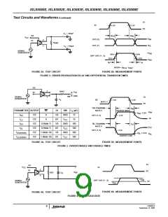
Electrical Specifications Test Conditions: V = 4.5V to 5.5V; Unless Otherwise Specified. Typicals are at V
= 5V, T = 25°C
A
CC
CC
(Note 4) (Continued)
TEMP
PARAMETER
SYMBOL
TEST CONDITIONS
= 1kΩ, C = 15pF, SW = GND (Figure 6),
(°C)
MIN
TYP
MAX UNITS
Receiver Enable to Output High
t
R
Full
-
10
30
ns
ZH
L
L
(Note 8)
Receiver Disable from Output Low
Receiver Disable from Output High
Time to Shutdown
t
R
= 1kΩ, C = 15pF, SW = V
(Figure 6)
Full
Full
Full
Full
-
-
10
10
30
30
ns
ns
ns
ns
LZ
L
L
L
CC
t
R
= 1kΩ, C = 15pF, SW = GND (Figure 6)
HZ
L
t
(Notes 9, 12)
R = 1kΩ, C = 15pF, SW = GND (Figure 6),
L
60
-
160
150
600
2000
SHDN
Receiver Enable from Shutdown to
Output High
t
ZH(SHDN)
L
(Notes 9, 11)
= 1kΩ, C = 15pF, SW = V (Figure 6),
CC
Receiver Enable from Shutdown to
Output Low
t
R
Full
-
150
2000
ns
ZL(SHDN)
L
L
(Notes 9, 11)
NOTES:
4. All currents into device pins are positive; all currents out of device pins are negative. All voltages are referenced to device ground unless
otherwise specified.
5. Supply current specification is valid for loaded drivers when DE = 0V.
6. Applies to peak current. See “Typical Performance Curves” for more information.
7. Keep RE = 0 to prevent the device from entering SHDN.
8. The RE signal high time must be short enough (typically <100ns) to prevent the device from entering SHDN.
9. Transceivers are put into shutdown by bringing RE high and DE low. If the inputs are in this state for less than 60ns, the parts are guaranteed
not to enter shutdown. If the inputs are in this state for at least 600ns, the parts are guaranteed to have entered shutdown. See “Low-Power
Shutdown Mode” section.
10. Keep RE = VCC, and set the DE signal low time >600ns to ensure that the device enters SHDN.
11. Set the RE signal high time >600ns to ensure that the device enters SHDN.
12. Guaranteed by characterization but not tested.
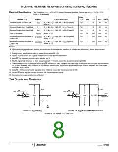
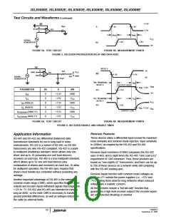
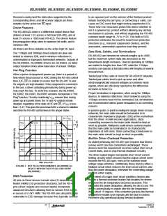
Test Circuits and Waveforms
R /2
L
375Ω
DE
DI
DE
DI
V
V
CC
CC
Z
Y
Z
Y
V
CM
R
= 60Ω
V
V
OD
L
D
D
OD
-7V to +12V
V
R /2
L
375Ω
OC
FIGURE 1A. V
OD
AND V
OC
FIGURE 1B. V WITH COMMON MODE LOAD
OD
FIGURE 1. DC DRIVER TEST CIRCUITS
FN6085.6
September 12, 2005
8

 INTERSIL [ Intersil ]