ISL83080E, ISL83082E, ISL83083E, ISL83085E, ISL83086E, ISL83088E
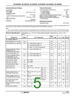
Absolute Maximum Ratings
Thermal Information
V
to Ground. . . . . . . . . . . . . . . . . . . . . . . . . . . . . . . . . . . . . . . 7V
Thermal Resistance (Typical, Note 3)
θJA (°C/W)
CC
Input Voltages
DI, DE, RE . . . . . . . . . . . . . . . . . . . . . . . . . -0.3V to (V
Input/Output Voltages
A, B, Y, Z . . . . . . . . . . . . . . . . . . . . . . . . . . . . . . . . . . -9V to +13V
A, B, Y, Z (Transient Pulse Through 100Ω) . . . . . . . . . . . . . ±25V
8 Ld SOIC Package . . . . . . . . . . . . . . . . . . . . . . . . .
8 Ld MSOP Package . . . . . . . . . . . . . . . . . . . . . . . .
14 Ld SOIC Package . . . . . . . . . . . . . . . . . . . . . . . .
Maximum Junction Temperature (Plastic Package) . . . . . . . 150°C
Maximum Storage Temperature Range. . . . . . . . . . .-65°C to 150°C
Maximum Lead Temperature (Soldering 10s) . . . . . . . . . . . . 300°C
(Lead Tips Only)
105
140
128
+ 0.3V)
CC
RO . . . . . . . . . . . . . . . . . . . . . . . . . . . . . . . . -0.3V to (V
Short Circuit Duration
+0.3V)
CC
Y, Z . . . . . . . . . . . . . . . . . . . . . . . . . . . . . . . . . . . . . . . Continuous
ESD Rating . . . . . . . . . . . . . . . . . . . . . . . . . See Specification Table
Operating Conditions
Temperature Range. . . . . . . . . . . . . . . . . . . . . . . . . . .-40°C to 85°C
CAUTION: Stresses above those listed in “Absolute Maximum Ratings” may cause permanent damage to the device. This is a stress only rating and operation of the
device at these or any other conditions above those indicated in the operational sections of this specification is not implied.
NOTE:
3. θ is measured with the component mounted on a high effective thermal conductivity test board in free air. See Tech Brief TB379 for details.
JA
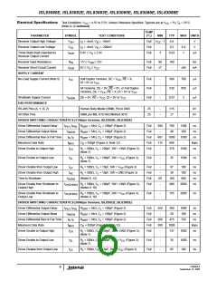
Electrical Specifications Test Conditions: V = 4.5V to 5.5V; Unless Otherwise Specified. Typicals are at V
= 5V, T = 25°C
A
CC
CC
(Note 4)
TEMP
PARAMETER
SYMBOL
TEST CONDITIONS
(°C)
MIN
TYP
MAX UNITS
DC CHARACTERISTICS
Driver Differential V
(no load)
V
V
Full
Full
Full
Full
Full
-
2
-
V
V
V
V
V
V
V
OUT
OUT
OD1
OD2
CC
-
Driver Differential V
(with load)
R
R
R
R
= 100Ω (RS-422) (Figure 1A)
= 54Ω (RS-485) (Figure 1A)
2.9
2.4
2.6
0.01
L
L
L
L
1.5
1.5
-
CC
-
= 60Ω, -7V ≤ V
≤ 12V (Figure 1B)
CM
Change in Magnitude of Driver
Differential V for
∆V
= 54Ω or 100Ω (Figure 1A)
0.2
OD
OUT
Complementary Output States
Driver Common-Mode V
V
R
R
= 54Ω or 100Ω (Figure 1A)
= 54Ω or 100Ω (Figure 1A)
Full
Full
-
-
2.85
0.01
3
V
V
OUT
Change in Magnitude of Driver
Common-Mode V for
OC
L
∆V
0.1
OC
L
OUT
Complementary Output States
Logic Input High Voltage
Logic Input Low Voltage
DI Input Hysteresis Voltage
Logic Input Current
V
DE, DI, RE
DE, DI, RE
Full
Full
25
2
-
-
-
-
0.8
-
V
IH
V
V
IL
V
-
100
-
mV
µA
µA
µA
µA
µA
µA
µA
mA
HYS
I
DE, DI, RE
DE = 0V, V
Full
Full
Full
Full
Full
Full
Full
Full
-2
-
2
IN1
IN2
Input Current (A, B)
I
I
I
= 0V or 5.5V
V
V
V
V
V
V
= 12V
= -7V
= 12V
= -7V
= 12V
= -7V
70
55
7
125
-
CC
IN
IN
IN
IN
IN
IN
-75
-
Output Leakage Current (Y, Z)
(Full Duplex Versions Only)
RE = 0V, DE = 0V, V
or 5.5V
= 0V
CC
125
-
IN3
IN3
-75
-
11
0
Output Leakage Current (Y, Z)
in Shutdown Mode (Full Duplex)
RE = V , DE = 0V, V
CC
or 5.5V
= 0V
20
-
CC
-20
-
9
Driver Short-Circuit Current,
I
DE = V , -7V ≤ V or V ≤ 12V (Note 6)
CC
-
±250
OSD1
Y
Z
V
= High or Low
O
Receiver Differential Threshold
Voltage
V
-7V ≤ V
≤ 12V
Full
25
-200
-
-90
20
-50
-
mV
mV
TH
CM
Receiver Input Hysteresis
∆V
TH
V
= 0V
CM
FN6085.6
5
September 12, 2005

 INTERSIL [ Intersil ]