ISL83080E, ISL83082E, ISL83083E, ISL83085E, ISL83086E, ISL83088E
Disabling both the driver and the receiver for less than 60ns
guarantees that the transceiver will not enter shutdown.
Low Power Shutdown Mode
These CMOS transceivers all use a fraction of the power
required by their bipolar counterparts, but they also include a
shutdown feature that reduces the already low quiescent I
to a 70nA trickle. These devices enter shutdown whenever
Note that receiver and driver enable times increase when the
transceiver enables from shutdown. Refer to Notes 7-11, at
the end of the Electrical Specification table, for more
information.
CC
the receiver and driver are simultaneously disabled
(RE = V
and DE = GND) for a period of at least 600ns.
CC
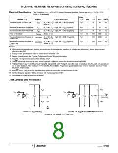
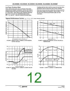
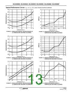
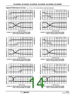
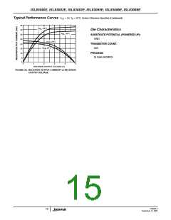
Typical Performance Curves V = 5V, T = 25°C; Unless Otherwise Specified
CC
A
90
80
70
60
50
40
30
3.4
3.2
3
R
= 100Ω
DIFF
2.8
2.6
2.4
2.2
2
R
= 54Ω
DIFF
20
10
0
0
1
2
3
4
5
-40
0
50
85
-25
25
75
DIFFERENTIAL OUTPUT VOLTAGE (V)
TEMPERATURE (°C)
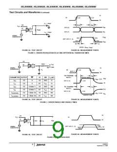
FIGURE 8. DRIVER OUTPUT CURRENT vs DIFFERENTIAL
OUTPUT VOLTAGE
FIGURE 9. DRIVER DIFFERENTIAL OUTPUT VOLTAGE vs
TEMPERATURE
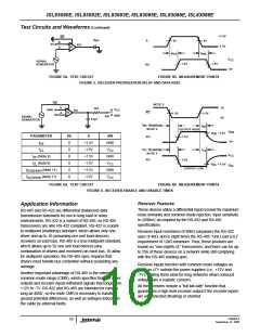
560
550
200
150
ISL83086E/88E
Y OR Z = LOW
HALF DUPLEX, DE = V , RE = X
CC
100
540
530
520
510
500
ISL83080E thru ISL83085E
50
0
HALF DUPLEX, DE = GND, RE = GND
FULL DUPLEX, DE = X, RE = GND
-50
Y OR Z = HIGH
-100
-150
ISL8308XE
-2
-40
0
50
85
-25
25
75
-7 -6
-4
0
2
4
6
8
10
12
OUTPUT VOLTAGE (V)
TEMPERATURE (°C)
FIGURE 10. DRIVER OUTPUT CURRENT vs SHORT CIRCUIT
VOLTAGE
FIGURE 11. SUPPLY CURRENT vs TEMPERATURE
FN6085.6
12
September 12, 2005

 INTERSIL [ Intersil ]