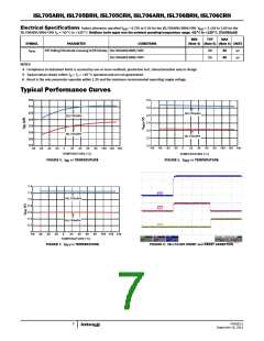
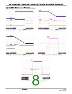
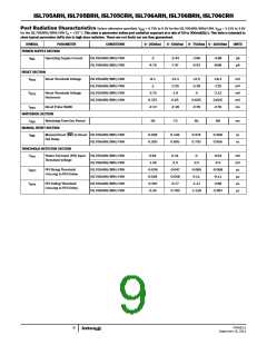
ISL705ARH, ISL705BRH, ISL705CRH, ISL706ARH, ISL706BRH, ISL706CRH
with VHB selected at 100mV. The closest standard value for R1 is
V
(EQ. 4)
PULL
---------------
R
=
124kΩ. Then next step is select the rising trip voltage (VTR) such
PULL
I
SINK
that:
VHB
⎛
⎝
⎞
⎠
-----------
(EQ. 6)
VTR > V
1 +
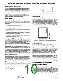
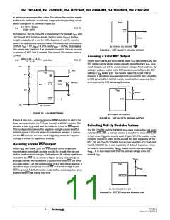
Adding Hysteresis to the PFI Comparator
PFI
V
DD
The PFI comparator has no built in hysteresis, however the
designer may add hysteresis by connecting a resistor from the
PFO pin to the PFI pin, essentially adding positive feedback to the
comparator (see Figure 20).
The rising threshold voltage is selected at 3.0V and R2 is
calculated by Equation 7.
VTR
1
1
⎛
⎝
⎞
⎠
⎛
⎝
⎞
⎠
⎛
⎝
⎞
⎠
-----------------------------
PFI
-------
-------
(EQ. 7)
R2 = 1 ⁄
–
–
(V
× R1)
R1
R3
Plugging in all the variables R2 in this example is 90.9kΩ again
this is choosing the closest 1% resistor. The final step is verify the
trip voltages.
V
DD
RST
PFO
R1
R2
1
R1
1
R2
1
R3
⎛
⎝
⎞
⎠
⎛
⎝
⎞
⎠
⎛
⎝
⎞
⎠
-------
-------
-------
(EQ. 8)
VTR = (V ) × R1
+
+
PFI
PFI
R1 × VDD
⎛
⎝
⎞
⎠
-------------------------
(EQ. 9)
VTF = VTR –
ISL705ARH
R3
The rising voltage, VTR is calculated as 2.98V and the falling
voltage VTF is calculated as 2.88V so 100mV hysteresis is
achieved.
R3
An additional item to consider is that the output voltage is equal
FIGURE 20. POSITIVE FEEDBACK FOR HYSTERISIS
to V , however according to the “Electrical Specifications” on
DD
page 6, the output of the PFI comparator is guaranteed to be at
The following procedure allows the system designer to calculate
the components based on the requirements and on given data,
least (V -1.5) volts. When you take this worst case into account,
DD
the hysteresis can be as low at 70mV.
such as supply rail voltages, hysteresis band voltage (V ), and
HB
reference voltage (V ).
PFI
Special Application Considerations
Using good decoupling practices will prevent transients (i.e., due
to switching noises and short duration droops in the supply
voltage) from causing unwanted resets and reduce the power-fail
circuit’s sensitivity to high-frequency noise on the line being
monitored.
The comparator only has two states of operation. When it is low,
the current through R3 is I = V /R3. When the output is high,
R3 PFI
I
= (V - V )/R3. The feedback current needs to be very
DD PFI
R3
small so it does not induce oscillations; 200nA is a good starting
point. Now two values of R3 can be calculated with V = 5V and
DD
= 1.25V; R3 = 6.25MΩ or 11.25MΩ, select the lowest value
V
PFI
When the WDI input is left unconnected, it is recommended to
place a 10µF capacitor to ground to reduce single event
transients from arising in the WDO pin.
of the two.
With R3 selected as 6.2MΩ (closest standard 1% resistor), R1
can be calculated as:
VHB
As described in the “Electrical Specifications” Table on page 7,
there is a delay on the PFO pin whenever PFI crosses the
threshold. This delay is due to internal filters on the PFI
comparator circuitry which were added to mitigate single event
transients. If the PFI input transitions below or above the
threshold and the duration of the transition is less than the delay,
the PFO pin will not change states.
⎛
⎝
⎞
⎠
-----------
(EQ. 5)
R1= R3
= 124kohms
V
DD
FN7662.0
September 15, 2011
12

 INTERSIL [ Intersil ]