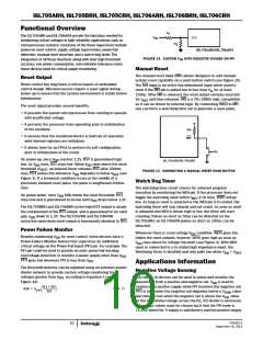
ISL705ARH, ISL705BRH, ISL705CRH, ISL706ARH, ISL706BRH, ISL706CRH
is at its maximum specified value. This allows the positive supply
to fluctuate within its acceptable range without signaling a reset
when configured as shown in Figure 16.
V
DD
R1(VPFI – Vtrip)
VDD – VPFI
---------------------------------------------
(EQ. 2)
R2=
RST
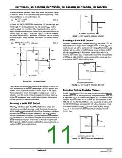
In Figure 16, the ISL705ARH is monitoring +5V through V and
DD
-5V through PFI. In this example, the trip point (V
) for the
TRIP
100kΩ
negative supply rail is set for -4.5V. Equation 2 can be used to
select the appropriate resistor values. R1 is selected arbitrarily as
100kΩ, V = 5V, V = 1.25V, and V
= (-4.5V). By plugging
ISL705ARH, ISL706ARH
DD PFI
TRIP
the values into Equation 2 as shown in Equation 3 it can be seen
FIGURE 17. RST VALID TO GROUND CIRCUIT
a resistor of 153.3kΩ is needed. The closest 1% resistor value is
154kΩ.
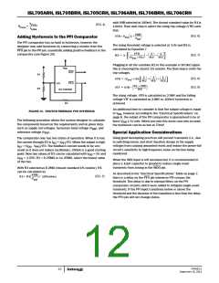
Assuring a Valid RST Output
On the ISL705BRH and ISL706BRH, when V falls below 1.2V, the
RST output can no longer source enough current to track V . As a
DD
result, this pin can drift to undetermined voltages if left undriven. By
adding a pull-up resistor to the RST pin as shown in Figure 18, RST
100k(1.25 – (–4.5))
-----------------------------------------------------
(EQ. 3)
R2=
= 153.3kΩ
DD
5 – 1.25
+5V
100k
V
DD
will track V below 1.2V. The resistor value (R1) is not critical
DD
R1
R2
MR
however, it should be large enough not to exceed the sink capability
of RST pin at 1.2V. A 300kΩ resistor would suffice, assuming there
is no load on the RST pin during that time.
100k
2N3904
PFO
PFI
V
DD
R1
300kΩ
RST
RST
-5V
ISL705ARH
FIGURE 16. ±5V MONITORING
ISL705BRH, ISL706BRH
FIGURE 18. RST VALID TO GROUND CIRCUIT
Figure 4 also has a general purpose NPN transistor in which the
base is connected to the PFO pin through a 100kΩ resistor. The
emitter is tied to ground and the collector is tied to MR signal.
This configuration allows the negative voltage sense circuit to
initiate a reset if it is not within its regulation window. A pull-up
on the MR ensures no false reset triggering when the negative
voltage is within its regulation window.
Selecting Pull-Up Resistor Values
The ISL705CRH and ISL706CRH have open drain active low reset
outputs (RST_OD). A pull-up resistor is needed to ensure RST_OD
is high when V is in a valid state (Figure 19). The resistor value
DD
must be chosen in order not to exceed the sink capability of the
RST_OD pin. The ISL705ARH has a sink capability of 3.2mA and
the ISL706CRH has a sink capability of 1.2mA. Equation 4 may
Assuring a Valid RST Output
be used to select resistor R
based on the pull-up voltage
When V falls below 1.2V, the RST output can no longer sink
PULL
DD
V
. It is also important that the pull-up voltage does not
current and is essentially an open circuit. As a result, this pin can
drift to undetermined voltages if left undriven. By adding a pull-down
resistor to the RST pin as shown in Figure 17, any stray charge or
leakage currents will be drained to ground and keep RST low when
PULL
exceed V
.
DD
V
PULL
V
V
falls below 1.2V. The resistor value (R1) is not critical however, it
DD
DD
should be large enough not to load RST and small enough to pull
RST to ground. A 100kΩ resistor would suffice, assuming there is no
load on the RST pin during that time.
R
PULL
RST_OD
ISL706CRH, ISL705CRH
FIGURE 19. RST_OD PULL-UP CONNECTION
FN7662.0
September 15, 2011
11

 INTERSIL [ Intersil ]